

Abstract
Moiré fringes are used throughout a wide variety of applications in physics and engineering to bring out small variations in an underlying lattice by comparing with another reference lattice. This method was recently demonstrated in scanning transmission electron microscopy imaging to provide local strain measurement in crystals by comparing the crystal lattice with the scanning raster that then serves as the reference. The images obtained in this way contain a beating fringe pattern with a local period that represents the deviation of the lattice from the reference. In order to obtain the actual strain value, a region containing a full period of the fringe is required, which results in a compromise between strain sensitivity and spatial resolution. In this paper we propose an advanced setup making use of an optimised scanning pattern and a novel phase stepping demodulation scheme. We demonstrate the novel method on a series of 16 nm Si–Ge semiconductor FinFET devices in which strain plays a crucial role in modulating the charge carrier mobility. The obtained results are compared with both Nano-beam diffraction and the recently proposed Bessel beam diffraction technique. The setup provides a much improved spatial resolution over conventional moiré imaging in STEM while at the same time being fast and requiring no specialised diffraction camera as opposed to the diffraction techniques we compare to.
Export citation and abstract BibTeX RIS
Introduction
Strain has become an essential ingredient in the functioning and performance optimisation of modern semiconductor devices. As an example, tensile strain increases the electron mobility in n-MOS devices while compressive strain increases the hole mobility in p-MOS devices [1–3]. With the ongoing trend of scaling down the size of transistors and the use of strain as a performance enhancing parameter, it is becoming essential to quantitatively measure strain at the nanoscale. Transmission electron microscopy based strain measurement methods provide the best possible spatial resolution, in principle down to the individual unit cell level. They can be broadly classified into diffraction and real space (imaging) based techniques. Diffraction based techniques like Nano-beam diffraction (NBD) offer a spatial resolution of 1–6 nm with a relative strain precision of 6 × 10⁻⁴ [3]. The spatial resolution is limited in an attempt to keep the diffraction discs as small as possible in order to avoid complications due to redistribution of intensities within the discs stemming from multiple elastic scattering processes. Nano-beam electron diffraction with precession (N-PED) circumvents the problem by averaging out diffraction patterns acquired at different tilt angles, thus partially cancelling the influence of multiple scattering. The intensity in the diffraction spots becomes more uniform, improving the precision to better than 2 × 10⁻⁴ [4, 5]. Recently, Bessel beam diffraction was shown to provide similar performance as N-PED but with minimal hardware complexity [6]. All diffraction techniques have a very good precision but are usually slow due to hardware limited acquisition speed restrictions and long data analysis. Moreover, the probe size on the sample can vary in a sensitive way on defocus and lens aberrations, which can imply a change in spatial resolution between experiments.
Real space based techniques like Dark field holography can measure strain with a very high spatial resolution (up to 3 nm), precision (0.2%), accuracy (0.1%) and wider field of view (up to 1 μm) using a bi-prism to interfere beams from the reference region and the strained region [7]. High resolution scanning transmission electron imaging with geometric phase analysis (GPA) has the ultimate spatial resolution as it is based on atomic resolution imaging of (a projection of) the crystal. In GPA, the spatial resolution and precision of the obtained strain map are inversely proportional and depend on the size of a mask applied in the Fourier space [8]. Typically, these methods have a lower field of view, but results are obtained fast due to rapid acquisition (a few seconds) and quick data analysis (less than a minute). STEM moiré strain mapping is an extension of the high resolution imaging which provides a higher field of view [9] at the expense of spatial resolution. The spatial resolution depends on the periodicity of the moiré fringes and is usually multiple times the crystal periodicity. In this paper, we attempt to extend the spatial resolution of the moiré strain analysis by combining it with phase shifting interferometry and demodulation techniques. We show that the precision obtained is approaching that of diffraction techniques while the spatial resolution can increase significantly and the acquisition and analysis time is lowered substantially.
STEM moiré theory
STEM moiré is a phenomenon caused by interference between a chosen sampling grid and the crystal lattice. The sampling grid is the periodic arrangement of the points sequentially visited by the STEM probe. The illuminated crystal lattice is then sampled at these points. We assume the STEM probe to be infinitely small here, which allows us to express the scanning grid as a 2D Dirac comb.
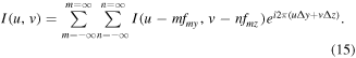
The continuous image of the sample (independent of specific imaging mode in STEM) can be expressed as an intensity variation of a detector signal (e.g. a high angle annular dark field detector) depending on the probe position 
Sampling in STEM is analogous to multiplication of this image function by a 2D Dirac delta comb 
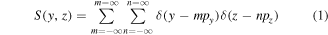
with  and
and  the spatial sampling step in y and z directions. We get a resulting discrete image:

In frequency space, this becomes a convolution of the Fourier transform (FT) of the image  with the FT of the 2D sampling grid which transforms to:
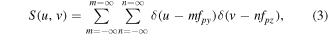
with, 
The discrete frequency spectrum of the sampled image is then written as
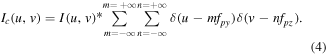
Note that we have taken the finite size of the sampling grid (the field of view) as a cut-off into the image spectrum rather than in the FT of the grid to keep the delta functions
This results in an infinite series of replicas with the central one occupying the frequency range ![$\left[\tfrac{-1}{2{p}_{y}},\tfrac{1}{2{p}_{y}}\right]\,\cup \left[\tfrac{-1}{2{p}_{z}},\tfrac{1}{2{p}_{z}}\right].$](https://content.cld.iop.org/journals/0268-1242/35/3/034002/revision2/sstab5da2ieqn7.gif) If the maximum frequency in the image
If the maximum frequency in the image  and
and  the sampling satisfies the Nyquist criterion and each replica is separated from all other replicas(figure 1(b)). In the case of under-sampling, aliasing happens, leading to the formation of moiré fringes by the replication of frequencies from outside the central portion into this region (figure 1(c)).

Figure 1. (a) Frequency representation of a periodic 2D signal. (b) Sampling with Nyquist criterion results in an infinite amount of replicas indicated by grey boxes with dimensions determined by the sampling frequency. (c) Moiré effect with sampling frequency lower than the highest frequency. The replication due to the finite sampling results now in a mixing up of the position of the frequency components which is best noted in the central replica marked in yellow. This mixing up is the essence of the moiré effect where frequencies appear different from what they really were without sampling. The frequencies get aliased and a high resolution frequency spectrum is now divided into smaller moiré windows with index (m, n) due to a lower sampling frequency in the moiré compared to a high resolution image. The arrow indicates the translation of frequencies into the new smaller central band.
Download figure:
Standard image High-resolution imageAs an example, we can assume an image made of two sinusoids (
 ) as shown in figure 1(a). A sampling frequency
  and
and  is chosen such that the Nyquist criterion is not satisfied, which results in the moiré effect (figure 1(c)). The yellow window represents the central replica with each red box an identical replication. The index of each window is represented by (m, n) and the frequencies that are outside the yellow window are translated into the yellow window by shifting the window over (
 ). For example, the frequency g1 is shifted one window down in v and one window left in u and so on [10]. This leads to a new apparent spatial frequency (the moiré frequency) within the central frequency band:


where  and
and  are the frequency components in y and z directions. For a projection image of Si or Ge along the [110] zone axis, we consider the y axis as the
 ![$\left[1\bar{1}0\right]$](https://content.cld.iop.org/journals/0268-1242/35/3/034002/revision2/sstab5da2ieqn18.gif) direction and the z axis along the [001] direction. The lattice distances for Si are different in these two directions
direction and the z axis along the [001] direction. The lattice distances for Si are different in these two directions  and
and  (figure 2(a)). This means, for any fundamental frequency in y and z directions,
  and
and  we have
  In conventional STEM, a square scanning grid is used and
  In general, this results in the creation of 1D moiré as m and n are not necessarily the same.
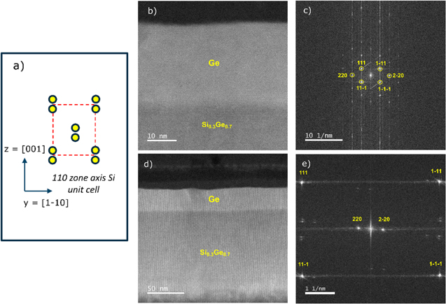
Figure 2. (a) Diagram of the unit cell of Si and Ge in [110] zone axis (b) HRSTEM image of the Si and Ge material and its corresponding diffractogram (c). (d) 1D moiré created on the Si and Ge material by undersampling at lower magnification and its corresponding diffractogram (e). The undersampling results in clear moiré fringes in (d) caused by only the {002} spots being replicated to rather low frequencies and a mixing up of the frequency components in (e). The moiré fringes are sentive to strain as seen by the slight wavyness and tilting of these fringes as a function of the location in the sample.
Download figure:
Standard image High-resolution imageFigure 2(d) shows an experimental image obtained with a square scanning grid, resulting in only one fringe direction to be visible while the other is too high in frequency. These 1D moiré fringes are easily observed for a probe aberration corrected instrument (the probe has to be smaller than the lattice spacing) and readily reveal strain as a slight change of the moiré fringes in different locations of the image.
The resulting distortion of the apparent symmetry by the formation of 1D moiré can be circumvented and a more interpretable situation occurs if the symmetry of the scanning grid matches the symmetry of the lattice by adjusting the scan pattern to obey:
with  the under-sampling factor >0.5. This can be done by adjusting the strength of the signals driving the scan coils. In this case, all frequencies transform as:
If m = n, this transform is an angle preserving scaling factor and the moiré fringes will have the same symmetry as the lattice. An experimental example is shown in figure 3(a).
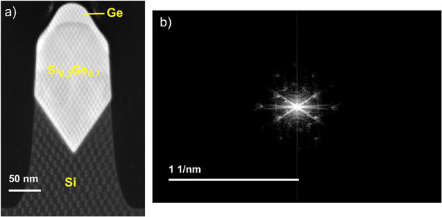
Figure 3. (a) 2D moiré fringes on a 100 nm FinFET cross section in [110] zone axis and its corresponding (b) diffractogram. Note the effect of local strain becoming visible as a distortion of the moiré fringe pattern in different locations of the sample.
Download figure:
Standard image High-resolution imageWhen strain occurs in the lattice, frequencies will shift by  and a relative shift of the diffracted spots can be obtained in the diffraction pattern (as in NBD). The strain in a particular direction is expressed as:
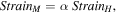
when under-sampling occurs, an apparent strain will appear in the moiré fringe as
The strain gets magnified by a boost factor  which makes it much more apparent as can be seen both in figures 3(a) and 4. This boosting is shape preserving (ε' stays parallel to
  ) only in the case where the scan grid matches the symmetry of the crystal and a situation is chosen where m = n. The strain boosting factor is plotted as a function of the under-sampling factor U showing how strain boosting is especially strong for low frequency moiré fringes. This also implies a hard trade-off between strain sensitivity and spatial resolution. In order to determine the frequency of the moiré fringe (related to the strain), one needs at least an area of the order of a period of the fringe.
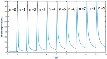
Figure 4. Strain amplification factor as a function of under-sampling. Note how strain magnification depends in a sensitive and nonlinear way on the choice of  and n is the moiré window (see
Download figure:
Standard image High-resolution imageAnother limitation comes from the fact that strain should not shift frequencies outside the central frequency replica. Otherwise m and n may differ for different areas of the sample leading to a much more complicated analysis (in fact a multivalued problem with non-unique solution). This limits the tolerable strain variation in a single image as strain amplification goes up. The change in the aspect ratio of the figures 3(a) and (b) is reflective of the scanning grid matching the symmetry of the lattice by adjusting the scan pattern.
Recovering the strain from moiré images: conventional way
Strain analysis of moiré STEM images is typically performed using GPA [11]. In this method a mask is used in the frequency domain to isolate the side bands around selected frequencies that carry the strain information. This selection mask determines also the spatial resolution that can be obtained and determines the signal to noise ratio in the resulting strain map. The larger the radius of the mask, the higher is the spatial resolution and the more noise enters the estimated strain map [11]. The mask radius is chosen to prevent selecting more than one diffraction spot at a time and is typically chosen smaller than half of the selected reference frequency. This reference lattice vector is used to demodulate the measured signal which then reveals the strain with respect to this reference.
Applying this method to moiré STEM images reveals the apparent strain which needs to be corrected back to the actual strain via equation (12) as shown in figure 5. As the strain magnification is significantly higher for low frequency moiré fringes, it is tempting to choose the undersampling as demonstrated in figure 5(a) where strain is readily apparent from the moiré image due to the boosting effect. The low frequency moiré fringes will however demand a small selection mask and result in poor spatial resolution. On top of this, multiple spatial frequencies, possibly having different m and n values, tend to cluster near the centre and can be very close to each other. This results in unwanted overlaps and the strain maps become unreliable, especially as each of these frequencies should be converted from apparent strain to actual strain with different scaling factors (figure 5).
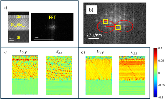
Figure 5. (a) 2D moiré on the 16 nm Fin long section and its corresponding FFT (b) GPA Masks used to isolate the regions in the FT. The yellow squares are the undesired interfering frequencies (c) normal strain  and
and  in the y and z directions obtained by GPA (d) comparing normal strain
  and
and  in the y and z directions obtained by GPA(using the same size of the mask) on moiré with quadtrature demodulation. Since the size of the mask used here is small, the spatial resolution is also reduced. A reliable strain map is obtained with the application of quadrature demodulation.
Download figure:
Standard image High-resolution imageIn order to overcome this difficulty and increase the practical usefulness of moiré strain mapping, we developed an alternative method that allows significantly suppressing other unwanted replica's.
Extending the spatial resolution with quadrature demodulation
If we could suppress the unwanted frequencies in the undersampled diffractogram, we could use a much larger mask size before demodulating the signal back to an image of the strain. This would result in higher spatial resolution and the suppression of artefacts. This is achieved by moiré phase stepping interferometry and Quadrature demodulation. The principle of moiré phase stepping interferometry is to phase shift the moiré fringes in different specific directions in repeated experiments.
If we shift the experimental scanning grid over  and
and  in y and z directions

and apply the Fourier shift theorem we get for the FT of the sampling grid

This results in phase shifting of the different components in the spectrum as
This equation shows that it is sufficient to shift the sampling grid by a reference lattice fringe spacing  and
and  to cause a
  phase shift of these moiré fringes in the under-sampled image.
Now, that we have the capability to phase shift the frequency components in the recorded moiré images by spatially shifting the sampling grid, we can apply an extended version of quadrature demodulation. Quadrature demodulation is commonly used in telecommunication (e.g. FM radio) [12] and allows to extract a given sideband of a modulated signal. In our case the 'carrier frequency' is a reference spatial frequency and the 'signal' is the strain or deviation with respect to this signal.
In this case we apply a 4 × 4 array of shifts of the scanning pattern, resulting in 16 independent and phase shifted moiré images. The applied shift can be represented as a 4 × 4 matrix S targeted to bring out the strain along 2 non-collinear reference frequencies  and
and 
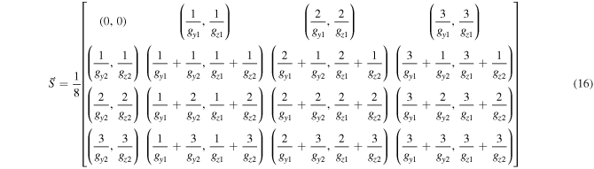
each index of the matrix can be written as:
As a spatial shift of 1/g implies a 2π phase shift, the shifts result in a complex factor that is applied to a specific frequency component in the frequency domain:

This means that we can single out any specific spatial frequency of interest by multiplying each sub-diffractogram  with the complex conjugate of the above matrix and then summing up over all k, l indices. This results in constructive interference of a selected frequency g while destructive interference occurs approximately for all other frequencies
with the delta function doing the actual demodulation. Converting this back to real space leads to the demodulated strain component with respect to the selected reference frequency

The selectivity improves with a  shifting matrix with increase in
  but this comes at the expense of an increase in the measurement time as
  A minimal choice would be n = 2, but we show in the experimental section that n = 4 provides a more realistic compromise. In fact, the suppression rate for any other frequency
  in the discrete Fourier space of the image can be calculated as
Ideally this suppression preserves frequencies close to the desired frequency as these carry the strain information but achieves a high suppression of frequencies that are further out.
Experiment
In order to implement the above mentioned idea in the transmission electron microscope, it is necessary to obtain software control over the probe scan engine. Making use of a custom built scan engine[collaboration Tence and Kociak [13]], we are able to freely programme the scanning pattern in an aberration corrected FEI Titan3 STEM instrument operating at 300 kV.
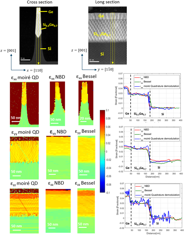
We start with a 16 nm Finfet test sample cut along the longitudinal section indicated in figure 6 to demonstrate the method. This sample consists of a silicon substrate on top of which a thick Si0.3Ge0.7 layer (∼110 nm) is grown epitaxially which is relaxed completely (due to a high aspect ratio, the structure relaxes by the formation of dislocations) and acts as the strain relaxed buffer (SRB). Then a thin layer (∼30 nm) of germanium is grown on top of SRB which is the channel of the FinFET. The Fins are 16 nm in width and are separated by silicon oxide (Shallow Trench Isolation, STI). The germanium channel FinFET material is developed by IMEC using the STI-first technique [14]. The cross section and long section of the Fins for the TEM analysis under low magnification STEM mode is shown in the figures 6(b) and (c). The V shape of the silicon substrate in the cross section is used especially to trap the defects in the SRB and prevent their propagation into the Ge channel [14].
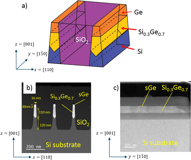
Figure 6. Schematic description of the FinFET (b) cross section and (c) long section of the 16 nm FinFET for the TEM strain analysis.
Download figure:
Standard image High-resolution imageThe scanning step-size is tuned to 17/16th of the lattice spacing of the silicon substrate in the y and z direction, i.e.  and
and  This results in a distorted under-sampled (U = 17/16 = 1.0625) moiré image that images the rectangular [110] projection of the silicon and germanium lattice as a square. This gives n = m = 1 and brings us into the central band with a strain amplification factor of
  (equation (12)).
For each scan point, 16 slightly shifted probe positions are visited with a shift vector given by equation (17) with  and
and  This results in a shift of the sampling probe by

with  and
and  chosen to be
  and
and  as sketched in figure 7.
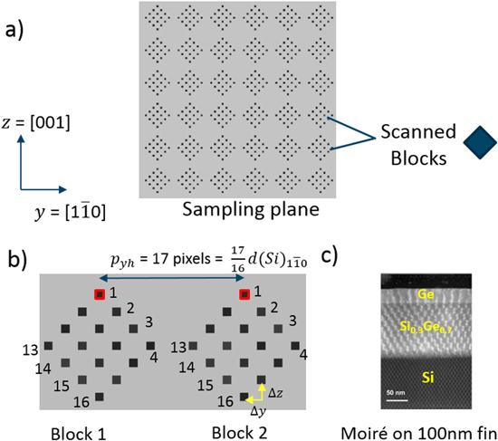
Figure 7. (a) Block scanning pattern overview. Black squares represent probe positions that are visited sequentially in blocks of 4 × 4 pixels. The order of the probe visiting positions inside each block is shown in (b). (c) Moiré image obtained by using only pixel 1 from each block, marked in red in (b). The pixel step size is  /16 in y direction and
  /16 in z-direction. This makes the pixel size for the moiré image
  th of the lattice spacing of Silicon(
 or
or  depending on the direction).
Download figure:
Standard image High-resolution imageThis results in 16 independent moiré images with shifted fringes. Applying the quadrature demodulation as explained above, we obtain the demodulated result for 

 as shown in figure 8.
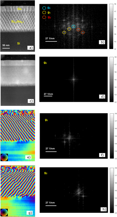
Figure 8. (a) Moiré on the 16 nm Fin longitudinal direction (b) and its diffractogram (c) demodulation to either g1 and g2 with a 4 × 4 shift matrix is shown as the phase of the demodulated wave in y, z-space (e), (g) and g0 with the real value in x, y-space (c) and the absolute value of amplitude in frequency space of g0, g1 and g2 (d), (f), (h). Note the selection of the desired frequencies while a strong suppression of the unwanted frequencies occur. There are two reflections in g1 and g2 corresponding to Si and Si0.3Ge0.7 material having different lattice spacings, but both are maintained after the quadrature demodulation process selecting Si as the reference lattice. This shows that the strained components remain while the other unwanted components are strongly suppressed.
Download figure:
Standard image High-resolution imageWe can calculate the suppression factor for each of the selected frequencies 

 (figure 9). Quadrature demodulation keeps the amplitude of the selected frequency while suppressing the other unwanted frequencies by destructive interference. The suppression factor of the undesired frequency is the damping factor that is applied to the undesired frequencies while maintaining the desired frequencies. Figure 9 shows that the effect of quadrature demodulation is similar to applying a 2D sinc function enhancement factor centred at the selected frequency while the other frequencies away from the selected frequency are greatly suppressed. As an example, if the frequency
  is selected, the suppression factor for the other two frequencies
  and
and  i.e. the ratio of the absolute value of amplitude of undesired frequency to that of the selected frequency in the Fourier space.

Figure 9. Quadrature demodulation scheme results in the extraction of the desired frequency bands. The figure illustrates the enhancement factor applied on three desired frequency sidebands g0, g1 or g2. The centres desired frequencies g0, g1 and g2 are highlighted with the red dot and the centres of undesired frequencies are highlighted in yellow.
Download figure:
Standard image High-resolution imageThis suppression of the undesired frequencies is highly beneficial when demodulating the reference frequency to zero as it allows the use of a very relaxed low pass filter (possibility to cover the full Fourier space of the image) to supress only far away components resulting in a much improved spatial resolution up to 1 nm.
To extract the 2D strain tensors we need to demodulate and extract strain with respect to two non-coplanar reference frequencies g1 and g2. The demodulated phase components Pg1 and Pg2 along both diagonal directions are shown as a phase plot indicating phase as colour (figures 8(e) and (g)) and amplitude as intensity in figure 8(c).
Strain is extracted using the formula derived from Hÿtch et al [11]. The displacement field is given as:

where,  and
and  are the y and z components of the displacement field
 and
and 
 and
and  are the y and z components of the two non-coplanar side bands of interest.
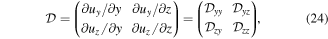
The distortion tensor  strain tensor ε and rotation tensor ω can be calculated from the gradient of the displacement field


Comparison to alternative techniques
In order to appreciate the performance of the present method, we compared it to the diffraction based strain measurement techniques like NBD and Bessel diffraction [3, 4, 6]. The analysis with these methods is applied to a 16 nm FinFet, which is a challenging structure in terms of the spatial resolution requirement but a realistic example of the current semi-conductor technology.
NBD was performed using a quasi-parallel probe with a beam convergence angle of ≈0.3 mrad at 300 kV using an FEI TITAN3 microscope. Bessel diffraction was performed at 300 kV using an aberration corrected FEI TITAN microscope and using an annular aperture in the C2 aperture plane. The convergence angle was chosen to be ≈6 mrad and this gives a diffraction pattern consisting of rings instead of discs (figure 10). Such lower convergence angle is chosen so as to limit the overlapping area between the rings. This improves the precision of the strain measurement but is traded off with the spatial resolution [6].
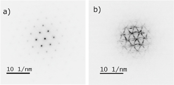
Figure 10. Diffraction pattern obtained with the NBD (a) and Bessel (b) diffraction techniques on Si at [110] zone axis. A spot diffraction pattern is obtained in NBD due to the quasi-parallel probe, while ring diffraction patterns are obtained in Bessel diffraction due to the annular aperture and a convergent probe.
Download figure:
Standard image High-resolution imageThe NBD and Bessel diffraction data are collected using a Gatan US1000XP CCD a camera. The NBD data is processed with the Epsilon 1.2.1.40 software from ThermoFischer scientific. The Bessel data is treated with a dedicated python based software, which is based on the autocorrelation of each diffraction pattern and subsequent extraction of the centre of the rings by background fitting and normalisation [6].
The strain maps were also obtained with the discussed phase stepping method and quadrature demodulation, offering an estimated spatial resolution of 2.8 nm (figure 11). Line profiles across the strain maps are averaged over 16 nm width perpendicular to the scan direction. Some scanning artefacts in the slow scan direction are still visible in e.g. the  strain line profile as stripe artefacts in the horizontal direction. These kinds of artefacts are typical for the STEM based strain methods and can be due to sample drift [15] and electromagnetic noise which results in instabilities of the probe position with respect to time. The precision of the proposed technique in the fast scan direction is estimated as 1.1 × 10⁻³ and the precision in the slow scan direction is 3.5 × 10⁻³. The precision calculated here is for the spatial resolution of 2.8 nm. Improved probe stability in the instrument and faster response of the scan coils (reducing the recording time) could further improve this performance in the future. Rotating the scan direction by 90° provides a direct way to trade precision performance from the y to z axis at the expense of an extra image acquisition.

Figure 11. (a) εyy strain maps obtained using GPA after performing the phase shifting and quadrature demodulation. The maps are obtained for different mask diameters covering up to half of the sampling frequency  (b) HAADF STEM moiré image of the Si and Ge sample used for strain analysis.
Download figure:
Standard image High-resolution imageThe typical trade-off between spatial resolution and precision in GPA is also present here as demonstrated in figure 12 for different low pass filtering choices. The advantage is that this choice can be made during post processing [16, 17]. The typical mask size for low pass filtering option is much higher in the case of the proposed moiré quadrature demodulation as opposed to applying GPA directly on moiré images. The reliability of strain maps has significantly increased alongside the spatial resolution. The precision of strain measurement observed for different mask sizes in figure 12(a) is 

 for mask sizes of
 and
and  (which leads to approximately ≈2.8, 1.7 and 1.2 nm spatial resolution) times the sampling frequency. This once again demonstrates the inverse nature of precision versus spatial resolution for GPA [17, 18].
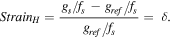
Figure 12. Strain maps obtained using moiré quadrature demodulation(QD), Bessel and NBD for the 16 nm FinFET on the cross section and long section of the Si and Ge samples providing an estimate of the complete 3D strain over the full structure. Strain profiles averaged over 16 nm horizontally as indicated by the yellow rectangle in the moiré images for all the three techniques mentioned above.
Download figure:
Standard image High-resolution image
Figure 12 provides a comparison of the strain maps obtained using moire quadrature demodulation and diffraction techniques like Bessel diffraction and nano-beam diffraction on a 16 nm FinFET. Analysing the line profiles of  reveals that the Ge and Si0.3Ge0.7 lattice distances are not the same as is expected for a fully strained Ge layer. This means there is relaxation of the Ge layer in the x direction. However, Ge conforms with the lattice distances of Si0.3Ge0.7 in the y direction as seen in the
  line profile. Since the relaxed Ge lattice is larger than that of Si0.3Ge0.7, it means that the Ge is compressively strained in the y direction. This results in an elongation in the z direction due to the Poisson effect [19] and can be seen in the
  line profile. The strain values computed on the Ge channel region with respect to bulk Ge (table 1) for the 16 nm FinFET reveals a uniaxial strain (y-axis) along the channel of the transistor. The strain is almost completely relaxed across (x-axis) the channel and there is a small tensile strain along the growth direction (z-axis). This trend is also confirmed after comparison with the diffraction based strain measurement techniques: NBD and Bessel diffraction [3, 6].
Table 1. Normal strain values in the germanium channel. The value is averaged over the germanium region and standard deviation is obtained for the complete Ge region.
| Technique | εxx Ge(across the channel) (%) | εyy Ge (along the channel) (%) | εzz Ge (Growth direction) (%) |
|---|---|---|---|
| Standard deviation over the full Ge area | |||
| Bessel diffraction | −0.17 ± 0.02 | −1.48 ± 0.02 | 0.18 ± 0.05 |
| Nano-beam diffraction | −0.20 ± 0.04 | −1.12 ± 0.02 | 0.17 ± 0.04 |
| Moiré quadrature demodulation | −0.22 ± 0.04 | −1.37 ± 0.03 | 0.12 ± 0.03 |
Table 1 shows a comparison of the strain values in the channel, refered to bulk Ge for moiré quadrature demodulation with NBD and Bessel diffraction.
The strain values are averaged over the complete Ge region and the standard deviation represented here is over the full region and does not represent the deviation for each individual pixel in the image.  This allows to make a fair comparison between methods which have a different spatial resolution and number of measurement points in the strain maps. The epitaxial conditions of growth of Ge on the Si0.3Ge0.7 SRB ideally leads to a compressive strain of −1.2% in the
  direction and a tensile strain of 0.34% in
  direction due to the Poisson effect, in accordance with the elastic theory for materials. Assuming that condition is fulfilled, we can estimate the accuracy for the Bessel diffraction, nanobeam diffraction and moiré quadrature demodulation for these measurements to be better than 0.2%, 0.1% and 0.2%. A better estimate of the accuracy needs further work on samples with well known strain levels.
Table 2 shows the comparison of the moiré quadrature demodulation technique with both diffraction-based techniques. The acquisition time and the analysis time per pixel is significantly lower for the moiré method as opposed to diffraction techniques. This is a direct consequence of the low frame rate that is present in any CCD camera as compared to the very fast readout possible with the HAADF detector used in the moiré method. Even the latest camera technology is still an order of magnitude slower and will probably remain so for the foreseeable future.
Table 2. Performance comparison of the three techniques evaluated in the strain free reference area: Bessel, NBD and moiré quadrature demodulation.
| Method | Spatial resolution | Precision over an area | Precision at nominal resolution | Field of view | Acquisition time (per pixel) | Analysis time (per pixel) | Total dose [ ] ] |
|---|---|---|---|---|---|---|---|
| Bessel diffraction | 1–3 nm |
 = 4.2 × 10⁻⁵ per 20 × 50 nm2 = 4.2 × 10⁻⁵ per 20 × 50 nm2  = 4.4 × 10⁻⁵ per 50 × 50 nm2 = 4.4 × 10⁻⁵ per 50 × 50 nm2  = 9.2 × 10⁻⁵ per 50 × 50 nm2 = 9.2 × 10⁻⁵ per 50 × 50 nm2 |

|
>500 × 500 nm2 | ≈150 ms | ≈124 ms | 4.6 × 10⁶ |
| Nano-beam diffraction | 1–3 nm |
 = 6.3 × 10⁻⁵ per 20 × 50 nm2 = 6.3 × 10⁻⁵ per 20 × 50 nm2  = 7.1 × 10⁻⁵ per 50 × 50 nm2 = 7.1 × 10⁻⁵ per 50 × 50 nm2  = 7.2 × 10⁻⁵ per 50 × 50 nm2 = 7.2 × 10⁻⁵ per 50 × 50 nm2 |

|
>500 × 500 nm2 | ≈25 ms | ≈156 ms | 0.7 × 10⁶ |
| Moiré quadrature demodulation | ≥0.7 nm |
 = 3.1 × 10⁻⁴ per 20 × 50 nm2 = 3.1 × 10⁻⁴ per 20 × 50 nm2  = 2.6 × 10⁻⁴ per 50 × 50 nm2 = 2.6 × 10⁻⁴ per 50 × 50 nm2  = 2.5 × 10⁻⁴ per 50 × 50 nm2 = 2.5 × 10⁻⁴ per 50 × 50 nm2 |

|
<500 × 500 nm2 (instrumental limitations apply due to scan coil response) | ≤0.1 ms | <4 μs or real time possible | 0.1 × 10⁶ |
The diffraction techniques involve 4D-STEM mechanism where each individual diffraction pattern is stored per pixel and hence it is also expensive in terms of data size in comparison to the moiré technique. Finally, The precision of the moiré quadrature demodulation technique is  computed for 3 nm spatial resolution and is in close agreement with the high resolution STEM and standard STEM moiré techniques [8, 20, 21] but with substantial increase in spatial resolution compared to standard moiré and a higher field of view compared to high resolution STEM. The boosting factor that moiré applies on the strain has an added advantage of effectively detecting small amounts of strain.
Due to longer acquisition and readout times, the total electron dose (number of electrons per area ![$[{{\rm{e}}}^{-}/{\rm{n}}{{\rm{m}}}^{2}]$](https://content.cld.iop.org/journals/0268-1242/35/3/034002/revision2/sstab5da2ieqn105.gif) ) impinged on the sample is significantly higher for the diffraction techniques. Shifting to a direct electron detector would significantly improve the signal to noise ratio and would allow for reducing the acquisition time with several orders of magnitude [22–24]. Nevertheless, it is expected that strain precision will scale with the square of the electron dose and we make a brief estimate for the setups presented here by comparing the obtained product of strain precision and the square root of the dose.
) impinged on the sample is significantly higher for the diffraction techniques. Shifting to a direct electron detector would significantly improve the signal to noise ratio and would allow for reducing the acquisition time with several orders of magnitude [22–24]. Nevertheless, it is expected that strain precision will scale with the square of the electron dose and we make a brief estimate for the setups presented here by comparing the obtained product of strain precision and the square root of the dose. ![$({P}_{d}=precision\times \sqrt{Dose}\,[\sqrt{{{\rm{e}}}^{-}}/{\rm{n}}{\rm{m}}]).$](https://content.cld.iop.org/journals/0268-1242/35/3/034002/revision2/sstab5da2ieqn106.gif) The
The  for NBD =
 ![$1.8\left[\sqrt{{{\rm{e}}}^{-}}/{\rm{n}}{\rm{m}}\right],$](https://content.cld.iop.org/journals/0268-1242/35/3/034002/revision2/sstab5da2ieqn108.gif) for Bessel =
for Bessel = ![$2.5\left[\sqrt{{{\rm{e}}}^{-}}/{\rm{n}}{\rm{m}}\right]\,$](https://content.cld.iop.org/journals/0268-1242/35/3/034002/revision2/sstab5da2ieqn109.gif) and for moiré quadrature demodulation technique =
and for moiré quadrature demodulation technique = ![$0.1\left[\sqrt{{{\rm{e}}}^{-}}/{\rm{n}}{\rm{m}}\right].$](https://content.cld.iop.org/journals/0268-1242/35/3/034002/revision2/sstab5da2ieqn110.gif) This shows that moiré quadrature demodulation technique is also highly dose efficient in comparison to the presented diffraction based strain measurement techniques although it is expected that upgrading to a more modern detector will significantly improve this performance metric for the diffraction methods.
This shows that moiré quadrature demodulation technique is also highly dose efficient in comparison to the presented diffraction based strain measurement techniques although it is expected that upgrading to a more modern detector will significantly improve this performance metric for the diffraction methods.
In summary, the moiré quadrature demodulation technique offers some of the important practical advantages over diffraction techniques such as fast data acquisition, no need for specialised high speed diffraction camera's, very fast data analysis and flexible choice of spatial resolution.
Conclusion
Standard strain mapping using GPA on moiré images suffers from reduced spatial resolution and interference from unwanted fringes and can lead to unreliable strain maps. A novel demodulation technique based on a generalisation of quadrature demodulation is proposed. We have shown that this significantly improves the spatial resolution and gives a more reliable and precise strain map at the expense of a somewhat longer acquisition as compared to conventional moiré imaging. The technique offers flexibility in the choice of field of view especially when compared to atomic resolution HR(S)TEM based methods. The method is near real-time in terms of acquisition and data analysis and provides the capability to trade spatial resolution for precision. Since moiré has the ability to boost strain values, it is highly sensitive and strain precision can be comparable to diffraction based methods without the need for specialised and slow diffraction cameras. We demonstrated the method on a relevant semiconductor device sample and compare its performance with diffraction based techniques.
Acknowledgments
The Qu-Ant-EM microscope and the direct electron detector used in the diffraction experiments was partly funded by the Hercules fund from the Flemish Government. This project has received funding from the GOA project 'Solarpaint' of the University of Antwerp. We would also like to thank Dr Thomas Nuytten and Professor Dr Wilfried Vandervorst from IMEC, Leuven for their continuous support and collaboration with the project.
Appendix
The lattice spacing and the atomic positions in the real space image have direct relation with the sinusoidal components in the FFT. This is not true for a diffraction pattern, which, has an inverse relation. Since we are dealing with GPA and real space images, we can directly relate the frequency components with the atomic positions as normally done in GPA.
The reference frequency is represented as  and the strained frequency as
 is the strain. After sampling with the STEM probe with frequency
  satisfying the Nyquist criterion, the digital frequency of the reference and strained area becomes
  and
and  This can also be called the strain calculated for the high resolution images which always satisfy the Nyquist criterion
So the obtained strain value is independent of the sampling frequency as long as the Nyquist criterion is satisfied.
Now, consider the moiré created using a different sampling frequency  that do not satisfy the Nyquist criterion, so the digital frequency obtained now is

 is the moiré window from which the frequency is translated (figure 1). Now, the strain obtained by moiré is
where  is the amplification factor.
So, the strain values for the moiré do depend on the sampling frequency and the moiré window from which the frequency is translated