

Abstract
We present a method for area selective deposition of 2D WS2 nanoribbons with tunable thickness on a dielectric substrate. The process is based on a complete conversion of a pre-patterned, H-terminated Si layer to metallic W by WF6, followed by in situ sulfidation by H2S. The reaction process, performed at 450 °C, yields nanoribbons with lateral dimension down to 20 nm and with random basal plane orientation. The thickness of the nanoribbons is accurately controlled by the thickness of the pre-deposited Si layer. Upon rapid thermal annealing at 900 °C under inert gas, the WS2 basal planes align parallel to the substrate.
Export citation and abstract BibTeX RIS
Abbreviations
| AFM | atomic force microscopy |
| ALD | atomic layer deposition |
| CVD | chemical vapor deposition |
| GIXRD | glancing incidence x-ray diffraction |
| PEALD | plasma enhanced atomic layer depositon |
| RIE | reactive ion etching |
| RBS | Rutherford backscatter spectrometry |
| SEM | scanning electron microscopy |
| TMA | trimethylaluminium |
| TMDC | transition-metal dichalcogenide |
| XPS | x-ray photoelectron spectroscopy. |
Due to their outstanding semiconducting properties, layered 2D transition-metal dichalcogenides (TMDC) such as WS2 are promising candidates for transistors with ultra-short channels below 10 nm. WS2 has a low dielectric permittivity, which is expected to reduce the parasitic short channel effects in comparison to silicon [1–3]. In addition, MX2 nanoribbons have lower permittivity than bulk films and thus, even better electrostatic control is expected [4, 5]. The deposition of monolayer and few-layered TMDCs are realized by thermolysis of liquid precursor or chemical vapor deposition (CVD) from the evaporation of elemental sulfur or gas phase precursors such as H2S or organic sulfides and solid metal-oxide precursors [6–10]. The deposition from volatile metal–halide or metal–organic precursors with CVD or atomic layer deposition (ALD) techniques were demonstrated by other groups already [11–25]. Those techniques typically show low deposition rates, e.g. a deposition time of more than one day was reported for a monolayer film formation [26]. In addition, metalorganic precursors present the risk of carbon incorporation in the semiconducting films, degrading their properties [27]. However, conventional Si-based CMOS fabrication methods cannot be applied easily to TMDCs since several key processing steps can damage the ultra-thin, sulfur-terminated transition-metal layers. For instance, plasma-based deposition and post-etch removal of masking layers by highly reactive strip chemistries can easily damage the ultra-thin TMDC layers [28–35]. Strong shifts in the threshold voltage Vth were observed, associated with the change from depletion to enhancement mode [32, 36]. Plasma-free patterning techniques can circumvent the damage and have already been demonstrated [37]. In the approach presented in this letter, we limit the patterning process to a sacrificial Si layer which is afterwards converted into WS2 layers, so that the WS2 is not exposed to plasma-based patterning, thus allowing for WS2 formation without plasma damage.
This letter describes the synthesis process for forming WS2 nano-ribbons on full 300 mm wafer scale, through selective replacement of a pre patterned a-Si nanoribbon by W, followed by in situ sulfidation with H2S as shown in figure 1(a).
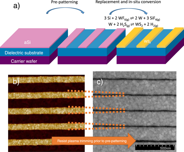
Figure 1. (a) Schematic of the aSi replacement process; (b) AFM scan on 70 nm WS2 lines with 130 nm space in between. (c) SEM images of 20 nm WS2 lines with 180 nm Al2O3 substrate in between, fabricated by resists trimming prior to aSi patterning.
Download figure:
Standard image High-resolution imageThe fabrication process is depicted in figure 1(a). A Si (100) 300 mm wafer was cleaned and coated with 10 nm Al2O3 deposited by ALD from trimethylaluminum (TMA) and ozone (O3) on 20 nm dry-deposited SiO2. This substrate was annealed at 1000 °C for 60 s in O2-rich atmosphere to crystallize the Al2O3 layer and strengthen it chemically. Afterwards, a 3 nm amorphous Si layer (aSi) was deposited by physical vapor deposition (PVD). The aSi film was selectively patterned towards the dielectric Al2O3 substrate layer by means of amorphous carbon (α-C) and SiOC hard mask. Immersion lithography with a wavelength of 193 nm was used to print lines of 70 nm width separated by 130 nm, thus yielding a 200 nm pitch. The a-Si film was patterned by reactive ion etching (RIE) using a SF6/CH2F2 mixture and the α-C was removed by O2/Cl2. Then the substrates were immersed in a O3/H2O mixture for 30 s and treated with 0.5% HF for 200 s to remove the SiO2 mask and to passivate the aSi with H, in order to prevent immediate oxidation in air [38]. Finally, the wafer was exposed to 14 cycles of sequential gas exposures of WF6, N2, H2S, and N2 for 15 s each. In the first step, the WF6 precursor reacts with the aSi layer. Depending on the process temperature either one of the following reactions occurs [39]:

or

The susceptor temperature was set to 450 °C and hence, the conversion proceeded according to (I). The Si-to-W conversion is very fast due to the high reactivity of WF6 with Si. The W is replacing Si which diffuses through the W layer due to segregation. For Si segregated on W, the sticking coefficient of WF6 is higher than on blanket Si, enabling a fast reaction [39].
The pressure in the reactor was held at 266 Pa at all times. The H2S pulse caused the in situ sulfidation of the metallic W layer. In contrast to Mo, W sulfidation from the metallic state is energetically more favorable and can be achieved at lower temperatures [40, 41]. Such a sulfidation reaction occurs as follows:

The Gibbs free energies at 450 °C, calculated by HSC Chemistry®, is –140 kJ mol−1 for reaction (III), indicating that the reactions could proceed voluntarily. The conversion of the Si-to-W with the in situ sulfidation on blanket films was demonstrated by our group earlier [11]. We have demonstrated that an oxygen-free Si layer can be used to reduce the gaseous WF6 precursor to metallic W, which can be easily sulfurized in situ by H2S at 450 °C. Those as deposited films improved in their quality upon rapid thermal annealing for 150 s in 10 sccm Ar gas flow in an AG Associates HEATPULSE 610 system.
The obtained nanostructures were inspected by scanning electron microscopy (SEM), atomic force microscope (AFM) ICON PT with a tip radius of 7 nm, Raman spectroscopy with a 633 nm laser, Rutherford backscatter spectrometry (RBS) with He+ beam of an energy of 1.523 MeV, and x-ray photoelectron spectroscopy (XPS) with a monochromatized Al Kα source (1486.6 eV) and a spot size of 400 μm.
Figure 1(b) shows an AFM scan of the 70 nm wide WS2 lines in the bright area and the darker 130 nm space exposing the Al2O3 underlying film. By applying a resist trimming process, prior to the dry etching of the hard-mask stack, it is also possible to narrow the aSi lines. As shown in figure 1(c), the final pattern can be trimmed down to 20 nm linewidth with reasonable linewidth roughness. The Al2O3 grain boundaries are visible in the bright area between the WS2 lines and introduces also steps into the WS2 nanostructures in figure 1(b), indicating that a the WS2 topography is governed to a large extend by the underlying Al2O3 surface topography. Those structures were also scanned by AFM and the roughness was evaluated. The roughness parameter RMS on top of the WS2 lines was 0.6 nm and in the spaces 0.3 nm. The latter one is similar as on blanket crystallized Al2O3 films, indicating that the dry etching of the aSi films did not increase the substrate roughness and resulted in minimal Al2O3 recess. The height of the nanoribbons was around 5.5 nm according to the AFM analysis.
The chemical composition of the WS2 was confirmed by spectroscopic analysis and the corresponding Raman and XPS spectra are shown in figure 2. The measurements were performed on arrays of WS2 lines. From the RBS measurements (not shown here), the number of atoms per area was extracted and a S/W ratio of 1.9 ± 0.2 was calculated, which is stoichiometric within the uncertainty. The XPS spectra were deconvoluted in an oxide and sulfide doublet. The as deposited material was 31% oxide and 69% sulfide and upon annealing the sulfide was quantified with 63%. This is different than in blanket films, in which the films were mainly WS2 with residual WO3 below 10%. The lines have many reactive edges of the multilayer structures exposed to air, which are prone to oxidation and could explain the difference to blanket films in which only the basal planes are in direct contact with air. No traces of unreacted Si above the XPS detection limit could be found in the WS2 lines, which indicates that the aSi is completely consumed during the replacement reaction (XPS spectra not shown here). Also, the WS2 Raman characteristic in-plane  and out-of-plane A1g vibrational modes are clearly visible on the WS2 arrays confirming the presence of the WS2 nanostructures. The frequency difference between the
  and A1g peaks of more the 68 cm−1 evidences the multilayer structure with more than five layers [42]. In between the lines, no WS2 could be detected with Raman spectroscopy, which is in agreement the absence of W on Al2O3 substrates from WF6 precursor [11].
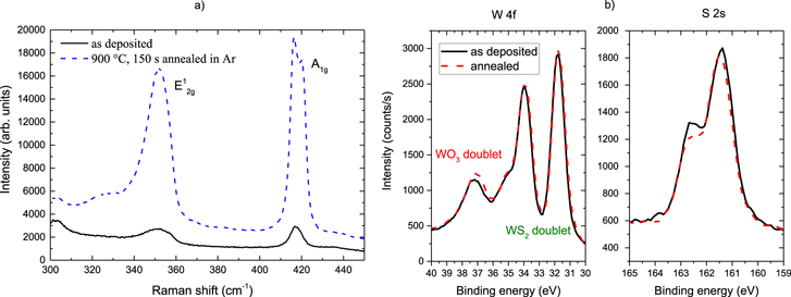
Figure 2. (a) Raman spectra taken with a spot size of approx. 1 μm on a WS2 array shown in figure 1. (b) W 4f and S 2s XPS spectra.
Download figure:
Standard image High-resolution imageFigures 3(a) and (b) show the cross-section TEM images taken perpendicular to the lines. The typical layered structure of TMDCs can be seen, where the dark layers represent the W atoms and the bright layers the S. These layers exhibit a low crystallinity: the basal planes in the as-deposited WS2 areas are randomly oriented and hence, they are only nanocrystalline. To achieve the desired horizontal basal plane alignment, the structures were annealed. Since MX2 films suffer from sulfur loss [43–48] during heat treatments in high vacuum or oxygen-containing environments, rapid thermal annealing at 900 °C for 150 s in Ar atmosphere was applied.

Figure 3. TEM cross section image with (a) small and (b) high magnification showing the 70 nm wide WS2 lines on the Al2O3; (c) after RTP at 900 °C for 150 s in Ar.
Download figure:
Standard image High-resolution imageThis annealing procedure yielded horizontal basal plane alignment in the structures, as can be seen in figure 3(c), indicating alignment towards the substrate occurred thanks to van der Waals forces. The WS2 presence and its crystallinity improvement have been also confirmed by glancing incidence x-ray diffraction (GIXRD) taken from blanket films, since the patterned samples provide only very small diffraction volume (figure 4). The WS2-characteristic peak around 14° represents the interlayer distance of the WS2 planes. Despite the broad peak due to the limited film thickness, the peak intensity is a measure for the crystallinity of comparable diffraction volumes. The intensity increase evidences the crystallization of the weakly ordered films and is comparable to the change observed in the TEM images. The interface between the WS2 and the Al2O3 underlayer is rough due to the polycrystalline character of both Al2O3 and WS2.

Figure 4. Grazing incidence x-ray diffraction peaks of the as-deposited WS2 and the 900 °C annealed WS2 films show the increase in crystallinity upon high-temperature treatment.
Download figure:
Standard image High-resolution image
In summary, a patterning-first fabrication technique for WS2 multilayer nanoribbons from a aSi layer and the gaseous precursors WF6 and H2S was developed. The aSi replacement and in situ sulfidation at 450 °C yields stoichiometric and randomly oriented WS2, which assemble in 2D structures upon rapid thermal annealing in inert gas. By eliminating the need for WS2 direct patterning, this process allows the creation of WS2 nanostructures down to 20 nm of high crystalline quality. Moreover, due to its self-limiting character, this technique is applicable to large substrates. This approach has the potential to control the WS2 layer number by adjusting the aSi thickness and the width by trimming the Si and enables the bottom-up growth of monolayer or few-layered structures with narrow width.
We believe that this deposition method by replacing pre-patterned sacrificial layers can be applied to other materials as well, and provides structures being appropriate to study size dependent electronic and morphological effects.
Acknowledgments
The authors thank Danielle Vanhaeren for the AFM characterizations, Yvo Crabbe for the SEM images, Johan Meersschaut for the RBS analysis, Thomas Nuytten for the Raman spectra measurements, Thierry Conard for the XPS characterizations, and Hugo Bender for the TEM cross-section images. This work was financially supported by a PhD grant of the Agency for Innovation by Science and Technology in Flanders (IWT).