

Abstract
Tunable transport properties and Fano resonances are predicted in a circular bilayer phosphorene nanoring. The conductance exhibits Fano resonances with varying incident energy and applied perpendicular magnetic field. These Fano resonance peaks can be accurately fitted with the well known Fano curves. When a magnetic field is applied to the nanoring, the conductance oscillates periodically with magnetic field which is reminiscent of the Aharonov–Bohm effect. Fano resonances are tightly related to the discrete states in the central nanoring, some of which are tunable by the magnetic field.
Export citation and abstract BibTeX RIS
1. Introduction
Since the discovery of graphene in 2004 [1], two dimensional (2D) materials have attracted great interest by researchers both from academia as well as industries owing to their intriguing properties. More and more 2D materials have been theoretically predicted and experimentally discovered such as graphyne [2], borophene [3], transition metal dichalcongenide (TMDC) [4], silicene [5], et al.
In recent years, phosphorene, a new 2D material, has been successfully fabricated from bulk black phosphorus (BP) [6, 7]. Phosphorene consists of a few phosphorus atom layers coupled by weak van der Waals interlayer interactions. Phosphorene is a promising 2D material due to its excellent mechanical, electronic, optical, and thermoelectric properties [6, 8–12]. BP is the most stable allotrope among the phosphorus group [13, 14], it possesses a direct band gap which can be tuned by the thickness of the film. The structure of BP is puckered which leads to the highly anisotropic properties in the band structure, electrical conductivity, thermal conductivity, and optical responses [7, 10, 15, 16] which is different from most of the widely studied 2D materials such as graphene, monolayer boron nitride, silicene, and TMDCs.
Many properties of phosphorene have been investigated both theoretically and experimentally, e.g., field transistor effect [6, 8], charged impurities [17], transport properties [7], excitons [15], optoelectronics and electronics [18–21], strain modification [10, 16], and a recent experimental demonstration of the crystalline anisotropy impacted phase coherent transport properties in BP field-effect transistor [22]. Among these studies, we note that an experiment carried out by Masih Das et al [23] demonstrates a practical way to sculpture phosphorus nanoribbons experimentally which provides the possibility of making a bilayer phosphorene nanoring (BPR) as proposed in this paper.
Ring geometries are particularly useful to study quantum interference effects such as special spin orbit interactions [24, 25], Aharonov–Bohm effect [26–28], and Fano resonances [29] arising from the interference between two transport paths in the nanoring. Fano resonances are important phenomena in quantum physics which has aroused a lot of attention in the pass few decades [30–32]. Fano resonances in graphene nanorings and graphene nanoribbons in the presence of a sidegate have been studied by Faria et al [29] and Petrovic et al [32], respectively. Fano resonances in the Mach–Zehnder–Fano interferometers are tunable by doping [33, 34].
However, Fano resonances in phosphorene nanorings remain unexplored. As both the transport properties of the phosphorene nanoribbons and the electronic properties of phosphorene nano structures are quite different to those of other 2D materials which makes it meaningful to investigate Fano resonances in phosphorene nanoring. In this work we theoretically investigate the electron transport properties in bilayer BPR utilizing the tight-binding (TB) method together with the recursive Green's function method. The ballistic conductance of nanorings with different incident energy, magnetic field are calculated. We find that there are two classes of peaks in the conductance: (1) resonance peaks due to electron wave interference in the leads of the structure, and (2) Fano peaks due to a spread (or bounded) local density of states (LDOS) as a consequence of the interference between discrete and continuum states.
The paper is organized as follows. In section 2, we present the TB model and give details about the calculation of the transport properties. In section 3, we show the transport and electronic properties of the BPR and investigate the transmission, DOS, LDOS of the BPR. The origin of the Fano resonances will be explained in this section. The effects of a perpendicular magnetic field will be demonstrated in section 4. Finally, we summarize our results in section 5.
2. Model and formulation
The lattice constants of bilayer phosphorene are a = 4.38 Å and b = 3.31 Å. There are eight phosphorus atoms in a bilayer phosphorene unit cell, the TB Hamiltonian for the BPR can be written as [18]

the summation runs over all the lattice sites of BPR,  (cj) is the creation (annihilation) operator of the electron at site i(j), and
  are the hopping energies, ten intra-layer and five inter-layer hopping links are included in our model [18]. The central part of the device is a circular ring, and in our numerical calculations we take the outer and inner dimeter of the ring equal 35.4 nm and 26.3 nm, respectively. The band gap of bilayer phosphorene given by this TB model is 1.15 eV with the valence band maximum and conduction band minimum located at −0.78 eV and 0.37 eV, respectively. When we apply a perpendicular magnetic field B to the BPR, and we use the Peierls substitution
  =
=  , where
  is the Peierls phase. In this work, we take the Landau gauge with vector potential
  and the magnetic field
  is homogeneous. The magnetic flux ϕ = Bab/2 through a plaquette is in unit of ϕ0 = ℏ/e.
The system is composed of a circular ring, i.e., the BPR and two semi-infinite leads. For the large size BPR, the Hamiltonian matrix HC is huge and difficult to solve directly, so we adopt the recursive Green's function algorithm in this work. The conductance is associated with the scattering properties of the conductor which is determined by the transmission probability via the Landauer Büttiker formula [35, 36]

where the Fermi energy Ef determines both the conductance G and transmission probability T. The conductance is in unit of  in the following part of this paper. The transmission probability T are determined by the the coupling between the conductor and the leads.

GCa is the advanced Green's function which is the Hermitian conjugate of the retarded Green's function GCr, and ΓL,R stands for the coupling between the conductor and the leads. In order to compute the Green's function of the conductor, we write the retarded Green's function as

where E is the quasi-particle energy and η is a positive infinitesimal number. HC is the Hamiltonian of the isolated conductor, ΣL,R are the self-energy terms which are defined as:

where HLC and HCR represent the coupling matrices. gL and gR are the surface Green's functions of the leads. The matrices ΓL,R can be easily obtained as:

From the Green's function, the LDOS at site i can be calculated as:

where Gi,i is the element of the Green's function at site i. The DOS is given in terms of the Green's function by
When we calculate the DOS of the whole system the contribution to the DOS from the semi-infinite leads are also considered when we calculate G0,0 and GN,N which are the Green's function of the first and last slice [37].
3. Fano resonances
In this paper we focus on the Fano resonances in BP nano devices, and investigate a BPR with a typical edge configuration, shape, and size. This typical BPR is schematically shown in figure 1 which is composed of two semi-infinite zigzag edged leads and one circular nanoring. The widths of the left and right leads are both 4.38 nm, the inner and outer diameter of the nanoring are 26.3 nm and 35.4 nm, respectively.

Figure 1. Schematic structure of phosphorene nanoring (green area) simulated in this work. The central part of the device is a circular ring, the outer and inner diameter of the ring are 35.4 nm and 26.3 nm, respectively. The width of the lead is 4.38 nm.
Download figure:
Standard image High-resolution imageFirst, the band structure of the leads is calculated, the conduction bands in the energy intervals between (0.4, 1.0) eV are shown in figure 2. The energy dispersions of the bilayer leads are quite different to those of single layer leads [26] because of presence of the interlayer coupling. For simplicity, in the rest of this paper we focus on the energy area between the two blue horizonal dashed lines and thus only one subband mode is occupied, which makes it easier to interpret the observed structures in the conductance of BPR.
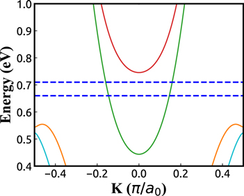
Figure 2. The energy dispersion of the BP lead with width 4.38 nm. In this work we focus on the energy interval between the blue horizonal dashed lines.
Download figure:
Standard image High-resolution imageIn figure 3, the conductance and the DOS of the nanoring are shown as function of the energy. In the conductance plot (figure 3(a)), there are two kinds of peaks: (1) antisymmetric peaks with a sudden change in the conductance, and (2) smooth broad peaks where the conductance varies smoothly with energy. The first kind of peaks are Fano resonance peaks and the second kind of peaks are resonance tunneling peaks. Two of the Fano resonance peaks are marked by a blue circle and one of the resonant tunneling peaks is marked by a green square which we will discuss in more detail. The DOS of the nanoring is shown in figure 3(b) for comparison. The DOS also exhibits two parts: (1) relatively small but continuum states which is seen as a background in the DOS, and (2) discrete sharp peaks. In this energy interval, only one subband in the lead is occupied so the contribution to the total DOS from the semi-infinite leads should be a continuum which is exactly the continuum DOS mentioned above. The discrete peaks are due to bound and quasi-bound states resulting from the coupling between the leads and the nanoring. Here we must emphasize the importance of the coupling between the leads and the nanoring as the eigenvalues of the nanoring detached from the leads are quite different from the system consisting of leads coupled with the nanoring.

Figure 3. (a) The conductance and (b) DOS of the nanoring. Conductance is in unit of G0, DOS is in arbitrary unit and scaled between zero and one. Two of the Fano resonance peaks and one of the interference peaks are marked by blue circular symptoms and a green square symptom, respectively.
Download figure:
Standard image High-resolution imageNow we address the origin of the Fano resonance peaks and the resonant tunneling peaks. From figure 3, we can see that the discrete DOS peak match very well with the position of the antisymmetric Fano resonance peaks in energy, i.e., where there is a DOS peak there is an antisymmetric Fano resonance peak which shows that the Fano resonance peaks are the results of the interaction of a discrete state with a continuum of propagating modes [31]. Notice that besides these Fano resonance peaks, there are also peaks without a corresponding DOS peak which we will show to be due to resonant tunneling.
The LDOS of the marked resonant tunneling peak and the corresponding antiresonance peak are shown respectively in figures 4(a) and (d). We can see that the LDOS of the resonant tunneling peak (figure 4(a)) and the corresponding antiresonance peak (figure 4(b)) are quite different from each other. The LDOS of resonant tunneling peak is spread over the whole nanoring while the LDOS of its antiresonance peak is spread over part of the nanoring. This phenomenon indicates that this conductance peak is due to the constructive interference between electron transport through the upper and lower part of the nanoring, i.e., resonant tunneling [26], and the dip is due to destructive interference. The LDOS of the first marked Fano resonance peak and its corresponding antiresonance peak are shown, respectively, in figures 4(b) and (e). The LDOS of the second marked Fano resonance peak and its corresponding antiresonance peak are shown respectively in figures 4(c) and (f). Obviously, the LDOS distributions of the Fano resonance peaks and the corresponding anti-resonance peaks are almost the same (but not exactly the same [31]), which indicates that the Fano resonance peaks are not the result of resonant tunneling but the result of the interplay between the leads and the ring. The LDOS corresponding to the Fano resonance peaks are localized in only part of the nanoring which implies Fano resonances are tightly related to the bound or quasi-bound states in the nanoring.
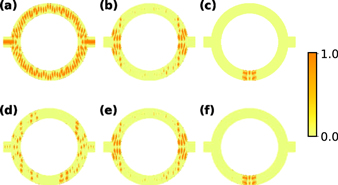
Figure 4. (a) and (d) are the LDOS corresponding to the broad peak and dip marked with the green square in figures 3(a), (b) and (e) are the LDOS corresponding to the first Fano peak and dip marked with blue circle in figures 3(a), (c) and (f) are the LDOS corresponding to the second Fano peak and dip marked with blue circle in figure 3(a).
Download figure:
Standard image High-resolution imageThe antisymmetric peaks shown in figure 3(a) can be described by the well known Fano curves [30, 31]. In contrast to a Lorentzian resonance, the Fano resonance exhibits a distinctly asymmetric shape with the following functional form:
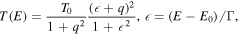
where T0 is the maximum value of the peak, E0 is the parameter which determines the position of the curve, Γ is the width of the resonance peak, and q is the shape parameter, i.e., q determines the line shape of the Fano peaks. Fano peaks with larger q posses a more symmetric line shape [31]. The quality factor (Q) of the Fano peaks are defined as [38]:

In figures 5(a) and (b), the Fano resonance peaks marked in figure 3(a) are perfectly fitted by the well known Fano curves [30, 31]. Figures 5(a) and (c) show the conductance and the corresponding DOS of the first Fano resonance peak, the energy is in units of meV. The position of this peak is E0 = 661.18 meV, the width parameter Γ = 5.36 × 10⁻³ meV and the shape parameter q = 4.05. When we refer to the corresponding DOS peak, the position of the DOS peak match very well with the Fano resonance peak. The Fano resonance peak and its corresponding DOS of the second marked peak in figure 3(a) are shown in figures 5(b) and (d). The position of this peak is E0 = 697.00 meV, the width parameter Γ =4.82 × 10⁻³ meV, but now with a very different shape parameter q = 56.47 which is one order of magnitude larger than the previous q. This difference originates from the distribution of the LDOS of the corresponding discrete states of the nanoring which can be inferred from figures 4(b) and (c). In figure 4(b), the LDOS spread over the nanoring, then the interference between the continuum states from the leads and the discrete states from the nanoring are strong which leads to and small q and a more anti-symmetric Fano peak. However, the LDOS in figure 4(c) is bounded in a small area, which will lead to a relatively larger q and a relatively more symmetric line shape. Notice that the position of the DOS peak also matches very well with the Fano resonance peak. This demonstrates that the Fano resonances are the result of the coupling between the continuum states from the leads and the discrete states from the ring. The quality factors of these two Fano peaks are 1.19 × 10⁵ and 1.44 × 10⁵, respectively. These high quality factors depend on both the position and the narrow band width of the Fano peaks.
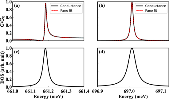
Figure 5. (a) and (b) show two Fano resonance peaks marked in figure 3(a). The Fano resonance peaks are fitted by the normalized Fano curve (red dashed curve). (c) and (d) are the DOS corresponding to the Fano resonance peaks shown in (a) and (b).
Download figure:
Standard image High-resolution image4. Tunable Fano resonances
In this section, we will study the transport properties in the presence of a perpendicular magnetic field. When a perpendicular magnetic field is applied to the nanoring, both the conductance and the DOS in the ring will oscillate periodically with the magnetic field, i.e., the Aharonov–Bohm effect [26–28]. In figure 6 the contour plot of both the conductance and the DOS in the presence of a perpendicular magnetic field are plotted, the period of oscillation can be approximated by the formula  ([26, 27]), here
 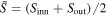 , which is the average area of the inner (Sinn) and outer (Sout) ring. The average area of the ring is 753.3 nm2, which results in
  . In figure 6(a), the conductance oscillate periodically with magnetic field, the period is about 5.4 T which matches very well with our theoretical prediction 5.48 T. The DOS shown in figure 6(b) oscillate synchronously with the conductance in the presence of a perpendicular magnetic field.

Figure 6. Contour plot of (a) conductance and (b) DOS of the nanoring as functions of a perpendicular magnetic field.
Download figure:
Standard image High-resolution imageAs mentioned above, there are two kinds of resonances in the considered energy interval; the origin of the Fano resonance peaks and the origin of resonant tunneling peaks are quite different as discussed above. However, both kinds of resonant peaks oscillate with magnetic field because of the Aharonov–Bohm effect in the nanoring. But there are some special peaks that do not change with the magnetic field both in the conductance plot (figure 6(a)) and the DOS plot (figure 6(b)). We attribute these peaks to localized edge states in the nanoring. Previously, in [19], localized edge states were found and shown not to be influenced by magnetic field as these states are highly localized at the edge atoms of the nanoring and the correlation length is much smaller than the magnetic length. However, the bulk states can be tuned by magnetic field [19], then the corresponding LDOS can also be tuned by magnetic field. Furthermore, interaction between the continuum states and the discrete states will lead to Fano resonance peaks, and therefore the magnetic field is also a useful way to tune the Fano resonances.
From figure 6 we can see that  (green dashed line in figure 6) is special as most peaks seem to disappeared. A zoom is shown in figure 7. We can see the conductance (figure 7(a)) is quite different from figure 3(a) as many peaks disappear due to the destructive interference in the presence of magnetic field. The DOS (figure 7(b)) is also quite different from the DOS shown in figure 3(b) as the bulk states of the nanoring [19, 28] will shift or disappear in the presence of magnetic field. Beside these differences, we can see that some of the peaks in figure 6 are preserved in figure 7 when B = 2.74 T. These similarities can be easily explained by referring to the LDOS plot in figures 4(b), (e) and (c), (f). The LDOS in figures 4(b) and (d) is spread over the nanoring and correspond to bulk states [19], while the LDOS in figures 4(c) and (f) are localized which correspond to edge states [19]. So when a perpendicular magnetic field (i.e.
  ) is applied, the Fano peaks (DOS peaks) corresponding to the bulk states disappear due to destructive interference, however the Fano peaks (DOS peaks) corresponding to the edge states are preserved.

Figure 7. (a) The conductance and (b) DOS of the nanoring for B = 2.74 T. Conductance is in units of G0, DOS is in arbitrary units and scaled between zero and one.
Download figure:
Standard image High-resolution image
5. Summary
We theoretically investigated the transport properties of a BPR by the recursive Green's function method. The central part of the nanoring leads to discrete states which interact with the continuum of propagating modes in the leads resulting in Fano resonances in the conductance. The Fano resonance peaks of the device match very well with the position of the DOS peaks, and the Fano resonance peaks are well fitted by the well known Fano resonance curves. The transport properties of the nanoring can be tuned by applying a vertical magnetic field, the conductance show Aharonov–Bohm effects. As the spread bulk states of the nanoring will oscillate with the magnetic field which makes it possible to tune the Fano resonance in the ring system. The qualities of the Fano resonances are high in BPR which lays a potential applications in electronic devices. In our study we used a typical BPR to demonstrate the physical origin of Fano resonances and the way to tune Fano resonances in BPR which paves the way for experimentalists to make use of the different resonances in the conductance for BP nano devices.
Acknowledgments
This work was supported by Grant No. 2017YFA0303400 from the National Key R&D Program of China, the Flemish Science Foundation, the grants No. 2016YFE0110000, No. 2015CB921503, and No. 2016YFA0202300 from the MOST of China, the NSFC (Grants Nos. 11504366, 11434010, 61674145 and 61774168) and CAS (Grants No. QYZDJ-SSW-SYS001).