
Abstract
In this contribution, we report a fundamental study of the factors that set the contact resistivity between metals and highly doped n-type 2D and 3D semiconductors. We investigate the case of n-type doped Si contacted with amorphous TiSi combining first-principles calculations with Non-Equilibrium Green functions transport simulations. The evolution of the intrinsic contact resistivity with the doping concentration is found to saturate at ∼2 × 10⁻¹⁰ Ω.cm2 for the case of TiSi and imposes an intrinsic limit to the ultimate contact resistance achievable for n-doped Si|amorphous-TiSi (aTiSi). The limit arises from the intrinsic properties of the semiconductors and of the metals such as their electron effective masses and Fermi energies. We illustrate that, in this regime, contacting heavy electron effective mass metals with semiconductor helps reducing the interface intrinsic contact resistivity. This observation seems to hold true regardless of the 3D character of the semiconductor, as illustrated for the case of three 2D semiconducting materials, namely MoS2, ZrS2 and HfS2.
Export citation and abstract BibTeX RIS

This is an open access article distributed under the terms of the Creative Commons Attribution 4.0 License (CC BY, http://creativecommons.org/licenses/by/4.0/), which permits unrestricted reuse of the work in any medium, provided the original work is properly cited.
Over the last technology nodes, the continuous reduction of the CMOS dimensions has been pushing the physical limits of the transistor into numerous ends. Consequently, a straightforward linear scaling of device dimensions can no longer cope with all the aspects of the CMOS transistor. For instance, the aggressive scaling of the transistor gate pitch requires that both the gate length and the source/drain (S/D) contact dimensions be reduced in size. This results in the gate, the sidewall spacers and the S/D contacts to compete continuously for space. In addition, the transistor gate length has also to follow a different scaling law and is kept as large as possible to ensure a proper electrostatic control. A direct consequence of this approach is the need to keep on decreasing the S/D contact resistance, which currently constitutes a new bottleneck in the scaling of modern CMOS. Aside from being able to reduce the physical dimensions of the contact, it is paramount to minimize the metal/semiconductor intrinsic resistivity which has now become a major roadblock to be conquered. Recently, the cumulated efforts of the scientific and engineering communities have substantially extended the physical limits of the S/D contact resistance thanks to the increase in the concentration of activated dopants in the semiconductors and to the engineering of their Schottky barrier. The latter is achieved by integrating metals with a weak Fermi level pinning at the interface with the semiconductor. As a result, contact resistivities as low as 2 × 10⁻⁹ Ωcm21 and 8.4 × 10⁻¹⁰ Ωcm22 have been reported for n-Si-aTiSi and p-Si30Ge70-aTiSi with dopant concentrations as high as 6 × 1020cm−3 and 1 × 1021cm−3.1,2 Aside from pushing the doping limits in conventional semiconductors, new materials are also being investigated which may allow better scaling and transport by virtue of their properties. Two-dimensional (2D) materials, especially transition metal dichalcogenides, have emerged as possible candidates in this regard22 for both MOSFET and tunnel based FET applications.23,24 Electrostatic doping in 2D materials also promises high carrier concentrations25 allowing for better transport. Although these accomplishments are impressive, little is known on the intrinsic limits that will ultimately determine the contact resistivity of conventional 3D and 2D semiconductors, and it remains unclear whether achieving even higher doping concentrations would be desirable or not.
In this contribution, we report a fundamental study of the contact resistivity between metals and highly doped semiconductors. We investigate the case of n-type doped Si contacted with aTiSi combining first-principles calculations with Non-Equilibrium Green functions transport simulations.4,5,28 We show that, whereas the metal/semiconductor intrinsic contact resistivity initially scales with the doping concentration, it is found to saturate at ∼2 × 10⁻¹⁰ Ω.cm2, as of a doping concentration of ∼5 × 1021 cm−3. From this concentration on, the electron injection is governed by Ohm's law. The analysis of contacts in 2D materials is a complex task due to the Van der Waals (vdW) layered nature and the lack of a proper understanding of the electron transport at the 2D/metal interface. It is nonetheless fundamental to learn if they obey the same limitations as 3D semiconductors. As an attempt to understand this point, we performed a qualitative study of their contact resistance with metals, assuming that they are side contacted and associated with a negligible Schottky barrier in the high doping limit. It turns out that, in high doping regimes, the electron injection does no longer depend on the barrier height set by the interface potential to be crossed. In turn, it becomes less sensitive to the chemical composition of the interface/degree of disorder and is limited by the intrinsic transmission probability of electrons being injected from the metal into the semiconductor. The latter depends on the value of the Fermi energy of the metal, on the effective masses of the metal and of the semiconductor3 and imposes an intrinsic physical limit to the contact resistance. We illustrate that, in this regime, contacting metals with a heavy electron effective mass help increasing the transmission probability and, hence, contribute to reducing the semiconductor-metal intrinsic contact resistivity.
Computational Methods
The molecular dynamic simulations were performed within the NVT canonical ensemble and the framework of the density functional theory (DFT) using a double ξ valence polarized basis6 set coupled with the exchange-correlation functional of Perdew, Burke and Ernzerhof [PBE],7 as implemented in the CP2K package.8 Core electrons were modeled by GTH pseudo-potentials9–11 with a plane wave cutoff of 750Ry (∼10204 eV) and a relative cutoff of 50Ry (∼ 680 eV) integrated with 5 sub-grids. Amorphous models of TiSi containing 50 atoms were generated using a melt and quench algorithm in which the crystal phase of TiSi12 was first melted at 2500K for 30 ps. The system is then cooled down passing three thresholds of 1000K, 600K and 300 K, each of them equilibrated for 9 ps. To avoid the building of strain artefacts at the Si(100)-aTiSi interface induced by the difference in lattice parameters between the materials, the (100) Si surface was rotated by 45 degrees. The in-plane lattice parameters of TiSi to be contacted were forced to match the Si substrate one, while the remaining dimension was defined to guarantee that the atomic density of the TiSi in its crystal phase is maintained during the melt and quench process. Once amorphized, both the lattice parameters and the atomic positions of the amorphous TiSi (aTiSi) model were completely minimized using a conjugated gradient minimization scheme. This approach ensures that the interface model used in this study has an interface strain mismatch lower than 1% between Si(100) and aTiSi, while keeping the atomic density of the disordered system realistic and the dimension of the interface models computationally accessible for the two-probe device simulations.
Finally, four different Si(100)-aTiSi two-probe device models containing 260 atoms were built and subsequently relaxed within the QuantumWise Atomistix ToolKit software package.4,5 The dimension of the silicon body was set to ∼5.5 nm to ensure that the width of the depletion layer generated by the doping concentration (ranging from 1 × 10²⁰ to 1022 |e|/cm3 n-Si(100)) is properly captured in the 'central' region of the device. The electronic temperature is set at 300 K. The thickness of the aTiSi layer in the central region is ∼2.3nm and corresponds to 2 repetitive units of disordered aTiSi (2.3 nm). The electrodes were built from ∼1.1 and ∼1.2 nm of bulk Si and aTiSi, respectively. The four models differ in the number of Ti atoms contacting the silicon substrate and their local coordination. Note that, though naive, these models lead to Schottky barrier heights close to the ones reported experimentally Aboelfotoh et al.29 and H. R. Liauh et al.30
The approach consists in solving the Kohn-Sham equations to evaluate the Hamiltonian of the system using DFT. The transmission spectrum is calculated using the Non-Equilibrium Green function (NEGF) method, and the current-voltage characteristics of the device are then computed within the framework of the Landauer-Büttiker formula,18 considering a ballistic transport process. To improve the description of the electronic bandgap, strongly underestimated by PBE, we used the Tran and Blaha exchange correlation functional13 with a c parameter value (c = 1.08) tuned to reproduce the bandgap of bulk Si combined with a norm-conserving (NC) pseudopotential and single ξ polarized (SZP) localized basis sets. The kinetic energy cutoff for the integration of the wave functions is set to be 75 Ha (2041 eV). We used a 21 × 21 × 100 Monkhorst-Pack integration k-point mesh in the device simulation part. The applied boundary conditions are periodic along the A, B directions and Dirichlet along the C one (Figure 1). The contact resistivity has been extracted by a linear fit of the current obtained upon the application of a potential bias in the linear regime (i.e. typically up to 0.1 V). The voltage applied spans from 0 to 0.2 V per steps of 0.025 V. Finally, the effective masses of the bulk metals were obtained by the second numerical derivation of their Fermi surface energy using a 60 × 60 × 60 Monkhorst-Pack integration k-point mesh and a Delaunay triangulation approach, as implemented in Paraview.14 The effective masses of 2D materials were extracted from the band structure computed using GGA-PBE with double-ς polarized basis and DFT-D3 correction,4,26 using one monolayer (ML), a Bi-Layer (BL) and a Bulk model.

Figure 1. Schematic illustration of one of the four n-Si(100)|aTiSi models used in this study. The Si and Ti atoms are colored in yellow and gray, respectively.
Results and Discussion
The disordered nature of amorphous metals such as TiSi makes the simulation of their interfaces with silicon complex. Indeed, the degrees of freedom at the interface in terms of local bond lengths, coordination number and composition make the development of an interface model challenging. In an attempt to capture these effects, we investigated the contact resistance of four different Si(100)-aTiSi interface models, in which the Ti and Si concentrations set in contact with the silicon substrate, their local coordination and bond lengths were varied. An atomistic model corresponding to the most stable energetic configuration is illustrated in Figure 1. All models lead to a current versus voltage (I.V.) characteristic curves similar to the one reported in Figure 2a, where a linear evolution of the current versus the applied voltage is obtained up to a bias of ∼0.1 V, after which the systems display a non-ideal linear behavior. The linear regime evolution was then used to extract the intrinsic contact resistance of the modeled interface. For instance, the intrinsic contact resistance of Figure 1 corresponds to 9.5 × 10⁻⁸ Ω.cm2 for a doping concentration of 1 × 10²⁰ |e|/cm3 and reflects the needs for the injected electrons to cross the interface potential set by the tail states19 present at the metal-semiconductor interface (Figure 2b). Interestingly, this model leads to contact resistances values relatively close to what has been recently measured experimentally by Hao et al.,15 as illustrated in Figure 3a. As expected, the contact resistance evolves linearly with the doping concentration to reach values as low as 1.8 × 10⁻¹⁰ Ω.cm2 for an active doping concentration of 1 × 10²² |e|/cm3. These findings are consistent with the recent demonstration of a sub 10−9 Ω.cm2 contact resistance for PMOS devices.20 Remarkably, the first-principles simulations also suggest that beyond this value the contact resistance should saturate, even for a completely unrealistic active dopant concentration of 1 × 10²³ |e|/cm3.
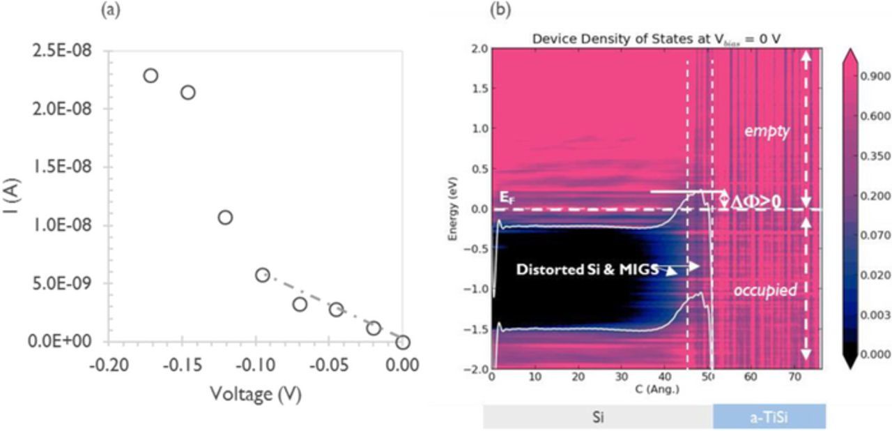
Figure 2. (a) Current versus voltage evolution computed for the energetically most stable n-Si(100)|aTiSi models using a Si n-type doping concentration of 1020 |e|/cm3. The dash-dotted line shows the linear regime used in the extraction of the contact resistance. (b) Corresponding evolution of the position dependent (X axis) Local Density Of States (LDOS) (Y axis) computed at a bias of 0 Volt for the energetically most stable n-Si(100)|aTiSi models. The X axis reflects the position along the main axis of the n-Si(100)|aTiSi interface (Figure 1). The zero of the energy is set to the Fermi level (EF). High and low density of states are colored in a hue spanning from pink to black respectively. The averaged Hartree potential is added as a guide line for the eyes and aligned on the top of the valence and bottom of the conduction band as continuous white lines. Vertical dashed lines point the position of the interface and the presence of MIGS states.
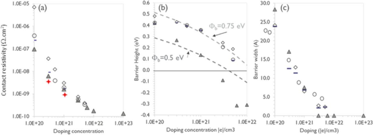
Figure 3. (a) Evolution of the contact resistance with respect to the doping concentration for four different n-Si(100)|aTiSi interface models. The gray triangle and red stars correspond to the values computed for the energetically most stable interface models and to the experimental values reported by Yu et al.15 for the same system, respectively. (b) Evolution of the associated energy barrier height (b) and width (c) to be crossed for an electron injection for the four different interface models. The evolution of the barrier height induced by image force lowering16 is added a visual guideline for two Schottky Barrier heights values 0.5 eV and 0.75 eV.
Further, the evolution of the contact resistance computed for different interface models underlines that the impact of the interface morphology/composition on the intrinsic contact resistance is strongly reduced upon large doping. While at 1 × 10²⁰ |e|/cm3 fluctuations of the intrinsic contact resistance vary up to 2 decades, they i) linearly decrease to reach a modulation factor 2 at 1 × 10²¹ |e|/cm3, ii) become almost undistinguishable as from 3 × 10²¹ |e|/cm3 to iii) finally saturate. Our simulations suggest that at high doping concentrations, the impact of the interface composition is strongly reduced and becomes less prominent. Consequently, the intrinsic contact resistance starts being dominated by the intrinsic properties of the metal and of the semiconductor. This is further confirmed by the evolution of the potential energy barrier height (Figure 3b) and its width (Figure 3c) to be crossed during the electron injection. Interestingly, the intrinsic Schottky barrier heights, 0.5 eV (for model 1) and 0.75 eV (for models 2 to 4) lie close to the experimental values reported for Si|Ti (0.6 eV) and Si|TiSi2 (0.5 eV)29 H. R. Liauh et al.30 (Figure 3b).
A closer analysis reveals that, while at low doping concentration, they both are strongly modulated by the image force potential generated at the metal-semiconductor interface16 (Figures 3b and 3c), an increase in the doping concentration leads to a transition of the dominant electron injection mechanism from a thermionic regime to an electron tunneling one. As from ∼3 × 10²¹ |e|/cm3 on, the height of the barrier and its width are so significantly reduced that an electron tunneling starts dominating the injection. As from mid-1021 |e|/cm3 on, there is no barrier anymore. The electron injection process then becomes dominated by the intrinsic interface transmission probability (Tp), which reflects the electron injection from the semiconductor into the metal and saturates. As analytically formulated by Baraskar et al.,3 the latter depends on bulk intrinsic material parameters such as the effective masses of the semiconductor (ms) and of the metal (mm), and their k vectors (kMZ and kSZ for the metal and semiconductor, respectively):
![Equation ([1])](https://content.cld.iop.org/journals/2162-8777/7/6/N73/revision1/d0001.gif)
Though this model relies on the free electron approximation, which leads to unrealistic prediction at high doping concentrations and hence cannot be directly compared to the first-principles ballistic results, it nonetheless brings useful insights. Indeed, Eq. 1 suggests that, once such a regime is reached, either no or a limited gain could be achieved by further increasing the doping concentration in the semiconductor and that other strategies should be pursued to further reduce the contact resistance. Baraskar et al.,3 formulated that once Tp is integrated over k space, and accounting for the energy distribution of the electronic levels in the metal (E) over the Fermi energy (Efs), the contact resistance in the ohmic regime (Ωc) takes the form:3
![Equation ([2])](https://content.cld.iop.org/journals/2162-8777/7/6/N73/revision1/d0002.gif)
Note that, in this formalism, the Fermi energy (Efs) should not be confused with the Fermi level energy, since the former corresponds to the difference in energy between the highest and lowest occupied electronic states in the free electron model, while the Fermi level is the total chemical potential of the electrons.
Keeping these aspects in mind, one can nonetheless establish a qualitative ranking of the potential of metals to maximize the transmission probability during the electron injection process since it depends on the Fermi energy (Figure 4c), on the effective masses in the metal (mm) (Figure 4b) and in the semiconductor (ms). Following this line of thoughts, Equations 1 and 2 offer a possible strategy to further reduce the contact resistance and suggest that metals with a high effective mass could be used to maximize the transmission probability of the electron injection. The crystal symmetry together with the orbital population of the metals lead to a rich modulation of their electronic properties at the Fermi level, their Fermi energy (Figure 4c) and is translated by a pronounced variation of their electron effective masses as evidenced in Figure 4b. Since the shape of the Fermi surface of a metal is set by its crystal symmetry, it ends up to be strongly anisotropic, as illustrated by the distribution of the electron effective masses computed for copper and ruthenium (Figure 4b). Interestingly, some metals such as bismuth can have an averaged effective mass as low as 0.047 me, while other ones, such as scandium can have an averaged electron effective mass as high as 29.43 me.

Figure 4. (a) Fermi surfaces (at 300K) of copper and ruthenium. The surfaces are colored with respect their direction dependent electron effective masses. (b) Evolution of the averaged effective masses computed for different metals. The empty white boxes correspond to the values reported in Reference 17, while the filled ones correspond to the averaged values computed using first-principles simulations. Since the Fermi surfaces of most metals are highly anisotropic, we report their edge values as error bars. (c) Evolution of the Fermi energy computed for different metals.
Assuming the case that all metals have the same Fermi energy, the computation of Tp (Eq. 1) at ksZ = 0 reveals that high effective mass metals helps in increasing the transmission probability at the Fermi level. For instance, going from a metal with a low effective mass such as W (mm = 0.73 me) to Sc (mm = 29.43 me), enhances the transmission probability by about 60% at 0.05 eV in the conduction band of silicon. This is translated into a reduction of the intrinsic contact resistance in the ohmic regime whenever the Fermi energy is allowed to vary from metal to metal (Figure 6). There is however a saturation effect as evidenced by the transmission probability (Figures 5a and 5b) and a strong dependency on i) the orientation of the Si substrate and ii) on confinement effects.21 For instance, the benefit of using a high effective mass metal is more pronounced for heavier transport effective mass (Figures 6 and 10). This is for instance obtained whenever the orientation of the channel is switched, going from a [100] transport direction (ms = 0.23 me)21 to a [111] one (ms = 0.41 me)21 or by narrowing the diameter of the Si channel, as reported in Reference 21 for highly confined [111] nanowires (ms = 0.53 me). In these cases, the contact resistivity further benefits from the increase in metal effective mass thanks to the enhanced transmission probability, as pointed out in Figure 10b. At higher energies, the transmission switches and consequently the contact resistivity increases for a higher effective mass metal. This effect is more pronounced for smaller effective mass semiconductors as shown in Figures 6 and 10. This observation holds true for 2D semiconductors as well (see Figures 7 to 9). Finally, these results suggest that contacting a faceted substrate, as it is the case in a Fin-FET technology, leads to an orientation dependent contact resistance.
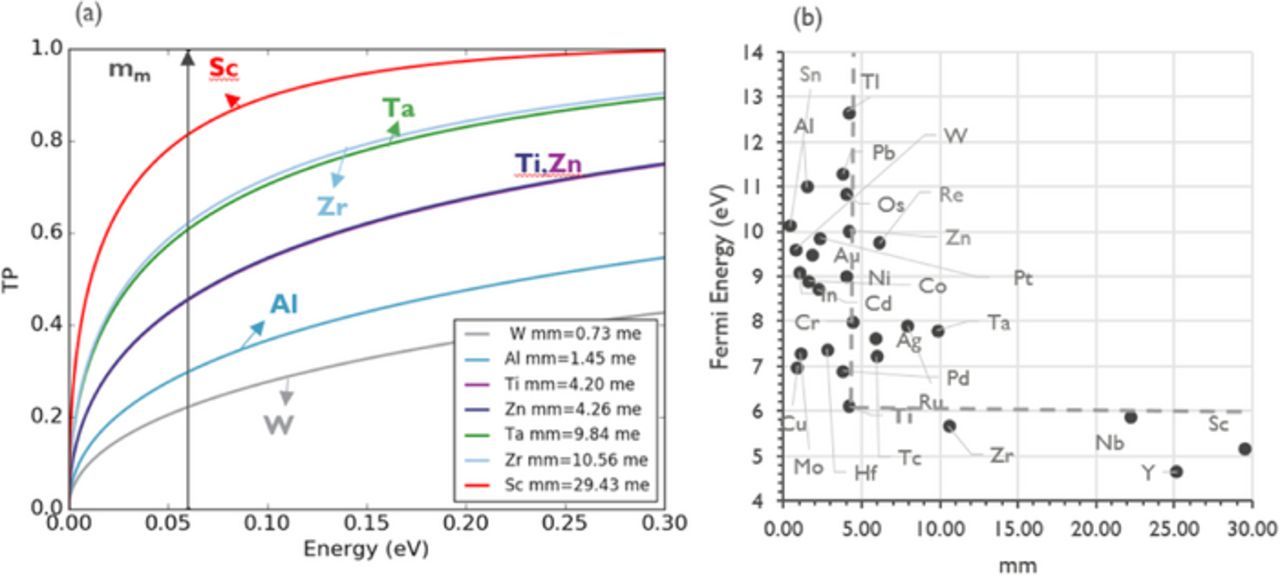
Figure 5. (a) Evolution of the transmission probability computed for different metals with respect to the conduction band energy of silicon within the formalism developed by Baraskar et al.3 Note that the transmission probability (TP) is computed at kST = 0 for the electron transport effective mass of Si along [100] (ms = 0.23 m0, as defined in Reference 21) and that the non-parabolicity of the conduction band of Si has been accounted for. (b) Distribution of the Fermi energy versus the averaged effective mass of metals.

Figure 6. Evolution of the contact resistivity computed for a doping concentration of 1 × 10²¹ |e|/cm3 using the formalism developed in Reference 3 for the electron transport effective mass of bulk Si along the [100] (0.23 me- light gray circles) and [111] directions (0.41 me-open circles)21 and for a 2nm diameter [111] nanowire (0.53 me-black circles).21
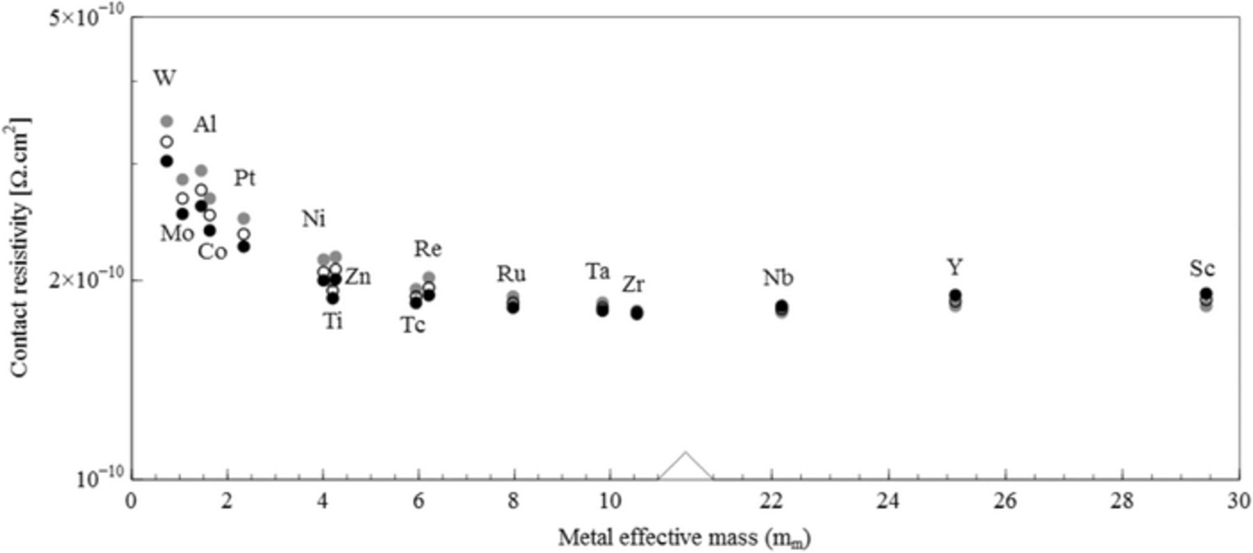
Figure 7. Evolution of the contact resistivity computed for a doping concentration of 6 × 10¹³ |e|/cm2 using the step barrier formalism of Reference 3. An effective mass of 0.526 m0 (black circles), 0.581m0 (open circles), 0.647m0 (light-gray circles) for ML, BL and Bulk MoS2 respectively was used.

Figure 9. Evolution of the contact resistivity computed for a doping concentration of 6 × 10¹³ |e|/cm2 using the step barrier formalism of Reference 3. An effective mass of 0.526 m0 (black circles), 0.302m0 (open circles), 0.296m0 (light-gray circles) for MoS2, HfS2 and ZrS2 respectively was used in the [010] direction.

Figure 10. Transmission probability (Eq. 1) computed for two extreme cases: a) Low effective mass semiconductor (ms = 0.041) in contact with a low effective mass metal (mm = 0.73 – W) (black line) and a high effective mass metal (mm = 29.43 – Sc) (gray line). The semiconductor conduction band (ECS) and the metal fermi level (Efm) are set at 0 eV. b) Transmission probability computed for a larger effective mass semiconductor (ms = 0.53- Si [111]) in contact with the same metals.
We extended the exercise to the case of the metal-2D semiconductor interface. Given that the real nature of this interface is still not clearly understood,27 we used a simple step barrier transmission model to account for it and to evaluate the resistivity limits of side contacted 2D semiconductors in their ohmic regime. Equations 1 and 2 were used to calculate the contact resistivity of MoS2 and Figure 7 provides a comparison of the resistivity of MoS2 in contact with different metals with the Fermi energies as reported in Figure 4. The contact resistivities are calculated at a n-type concentration of 1 × 10²¹|e|/cm3, which is roughly equivalent to a 2D doping of 6 × 10¹³ |e|/cm2 assuming a monolayer thickness of ∼ 6 Å (i.e. the thickness of the 2D material and of the van der Waals gap) for all the 2D materials considered. This value is chosen as being the ultimate limit of the doping concentration that can be used within this formalism before breaking the boundaries of the validity of the approximations used in Equations 1 and 2. The use of higher doping concentrations would introduce unrealistic offsets between the Fermi-level and conduction band in degenerate semiconductors.
As observed previously for Si, the contact resistivity of MoS2 is reduced with the increase of the metal effective mass and shows a saturation effect with the doping concentration. We focus on a 6 × 10¹³ |e|/cm3 doping in Figures 6–9 to probe the contact resistivity in a high doping regime. Note that the Fermi energies do not follow the evolution of the effective masses (Figures 6–9) and we do not see a smooth contact resistivity curve with metal effective masses. The modulation of the semi-conductor effective mass, going from Si to MoS2, has a larger impact on the contact resistivity than a variation in mm. Changing the orientation of the channel in Si, when going from [111] to [100], decreases the electron effective mass and leads to a rise of the contact resistivity for metals with heavy mm, as illustrated in Figure 6. This is also observed in MoS2 (Figure 8), where its relatively small effective mass compared to the HfS2 and ZrS2 ones, leads to a large contact resistivity (see Figure 10a). In this case, the value of the semiconductor electron effective mass leads to a low transmission probability (and thereby to an increase in contact resistivity). Switching to larger values leads to an improved transmission probability (Figure 10b). Intuitively, this can be pictured as the balance achieved by the system between the charge density injected by the density of states of the semiconductor in the metal, and the capability of its electronic structure to accommodate the injected electrons.
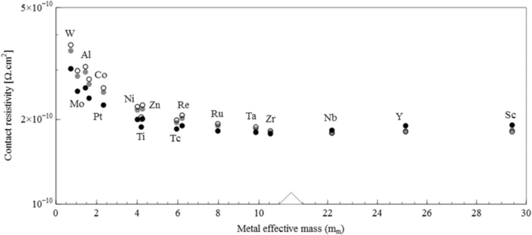
Figure 8. Evolution of the contact resistivity computed for a doping concentration of 6 × 10¹³ |e|/cm2 using the step barrier formalism of Reference 3. An effective mass of 0.526 m0 (black circles), 0.701m0 (open circles), 0.654m0 (light-gray circles) for MoS2, HfS2 and ZrS2 respectively was used in the [100] direction.
A similar trend is observed for other 2D materials such as HfS2 and ZrS2. As illustrated for the case of silicon, the orientation of the substrate transport direction has an impact on the contact resistance. Indeed, unlike MoS2, which has an isotropic effective mass in its conduction band, other 2D materials like HfS2 and ZrS2 have highly anisotropic electron effective masses and therefore they adopt a different contact resistance (Figures 8 and 9) depending on the chosen effective masses ([100] or [010] directions). This aspect is especially important since the interfaces with 2D materials are per nature driven by VdW forces, they can hence easily adopt different orientations when set in contact with other materials, leading to a source of variability for the contact resistances, as illustrated in Figures 8 and 9. Nevertheless, the expected impact on contact resistivities is modest with a modulation by a maximum factor of ∼2–3 times, while moving from a lower effective mass metal to a higher one.
Conclusions
We reported a fundamental study of the factors that set the contact resistivity between metals and highly doped semiconductors. We investigated the case of n-type doped Si contacted with aTiSi combining first-principles calculations with Non-Equilibrium Green functions transport simulations and showed that, whereas the metal-semiconductor intrinsic contact resistivity initially scales with the doping concentration, it is found to saturate at ∼2 × 10⁻¹⁰ Ω.cm2, as of a doping concentration of ∼5 × 1021 cm−3. For MoS2, the contact resistivity was found to saturate around 2 × 10⁻¹⁰ Ω.cm2 at ∼6 × 10¹³ |e|/cm2 on an average. For such concentrations, the electron injection is governed by Ohm's law. It turns out that, in such high doping regimes, the electron injection does no longer depend on the barrier height set by the interface potential to be crossed. In turn, it becomes less sensitive to the chemical composition of the interface/degree of disorder and is limited by the intrinsic transmission probability of electrons being injected from the metal into the semiconductor. The latter depends on the Fermi energy of the metal and on both the effective masses of the metal and of the semiconductor and imposes an intrinsic physical limit to the contact resistance. In this regime, contacting metals with a heavy electron effective mass is favorable to increase the transmission probability and, hence, to reduce the semiconductor-metal intrinsic contact resistivity independently of the 2D or 3D nature of the semiconductor. However, the resulting effect is rather limited and deteriorates for semiconductors with low effective masses.
Acknowledgments
The authors thank the imec core CMOS program members, the European Commission, its TAKEMI5 ECSEL research project and the local authorities for their support.
ORCID
A. Dabral 0000-0002-1761-8814
H. Yu 0000-0002-1976-0259