

Abstract
Recent efforts in the development of YBa2Cu3O7−x (YBCO) coated conductors are devoted to the increase of the critical current Ic in magnetic fields. This is typically realized by growing thicker YBCO layers as well as by the incorporation of artificial pinning centers. We studied the growth of doped YBCO layers with a thickness of up to 7 μm using pulsed laser deposition with a growth rate of about 1.2 nm s−1. Industrially fabricated ion-beam textured YSZ templates based on metal tapes were used as substrates for this study. The incorporation of BaHfO3 (BHO) or Ba2Y(Nb0.5Ta0.5)O6 (BYNTO) secondary phase additions leads to a denser microstructure compared to undoped films. A purely c-axis-oriented YBCO growth is preserved up to a thickness of about 4 μm, whereas misoriented texture components were observed in thicker films. The critical temperature is slightly reduced compared to undoped films and independent of film thickness. The critical current density Jc of the BHO- and BYNTO-doped YBCO layers is lower at 77 K and self-field compared to pure YBCO layers; however, Ic increases up to a thickness of 5 μm. A comparison between films with a thickness of 1.3 μm revealed that the anisotropy of the critical current density Jc(θ) strongly depends on the incorporated pinning centers. Whereas BHO nanorods lead to a strong B∣∣c-axis peak, the overall anisotropy is significantly reduced by the incorporation of BYNTO forming a mixture of short c-axis-oriented nanorods and small (a–b)-oriented platelets. As a result, the Jc values of the doped films outperform the undoped samples at higher fields and lower temperatures for most magnetic field directions.
Export citation and abstract BibTeX RIS
1. Introduction
In recent years, significant effort has been made to improve the functional properties of REBa2Cu3O7−x (RE = Y, Gd etc) based coated conductors in order to meet the requirements for applications in motors, generators, cables or high field coils. In general, coated conductors are realized on highly textured metal-based templates, which are routinely prepared nowadays in a length of several hundred meters [1]. One of these template technologies is the preparation of biaxially aligned buffer layers using ion-beam assisted deposition processes [2]. In this case, an additional off-normal ion beam is used to imprint a strong texture in such a buffer during growth. We used a stainless steel substrate covered with a biaxially textured YSZ layer for our studies, which was prepared by the so-called alternating beam assisted deposition (ABAD) scheme, more details can be found in [3].
Recent efforts in the development of REBa2Cu3O7−x coated conductors are directed to increase the critical current Ic in magnetic fields. A first option for a considerably increased overall current is to use thicker superconducting layers. However, a significant reduction of the critical current density Jc is typically observed for increasing thickness, which is mainly due to the changes in the microstructure as shown for YBa2Cu3O7−x (YBCO) films grown by pulsed laser deposition (PLD) [4]. We showed recently an increase of Ic up to a thickness of about 3 μm in thick YBCO layers grown on ABAD-YSZ templates [5]. Exceeding this thickness, a significantly increased surface roughness, arising from a high volume fraction of pores as well as from the formation of misoriented YBCO grains, leads to a limitation of the current transport. A similar reduction of Jc was also found for thick layers prepared with different deposition techniques such as metal-organic chemical vapor deposition (MOCVD) [6]. Nevertheless, Jc values up to 3 MA cm−2 at 77 K, self-field have been reported for 2.2 μm thick (Gd,Y)Ba2Cu3Ox films using MOCVD with additional Zr additions [7].
A second focus of current investigations is to improve the critical current density in magnetic fields by the inclusion of artificial pinning centers. Among the studied materials so far, BaMO3 (M = (transition) metal, e.g. Ir [8], Hf [9–11], Sn [12], Zr [13–15]) perovskites can self-assemble into cYBCO-oriented rods or (a–b)YBCO-parallel platelets with typical diameter or thickness of several nanometers depending on growth velocity, temperature, secondary phase amount and local grain or global substrate misorientations [16]. The resulting distribution of such second phase particles has a specific influence on the critical current anisotropy Jc(θ). BaHfO3 (BHO) has shown a low decrease in Tc and the smallest nanorod diameter [17], making it a suitable candidate for pinning enhancements also at lower working temperatures. Double-perovskites as Ba2YNbO6 (BYNO) [18, 19] and Ba2YTaO6 (BYTO) [20, 21] also offer a negligible Tc decrease and a fine pinning center distribution due to the low mobility of the large Nb, Ta ions. Extremely straight nanorods were found for the inclusion of the mixed compound Ba2Y(Nb0.5Ta0.5)O6 (BYNTO) in YBCO thin films resulting in superior pinning force density values and high matching fields [22–24].
The scope of this paper is to give an overview of our recent efforts in the basic study of the influence of different dopants on the structural and superconducting properties of thick YBCO films deposited on reel-to-reel produced ABAD-YSZ tapes by PLD, performed within the EuroTapes project. Only small samples with a maximum length of 20 mm having a doping of either 5 mol% BYNTO or 6 mol% BHO are studied in this work. All samples are prepared in a standard deposition setup with stationary substrate. In general, the structural and superconducting properties are influenced by a number of deposition parameters. In this paper, we will focus on doped YBCO films with a thickness of more than 1 μm grown with an average deposition rate of about 1.2 nm s−1 using a laser repetition rate of 10 Hz in order to study if the incorporation of artificial pinning centers has any influence on the thickness dependence of Jc. The influence of other deposition parameters, such as deposition temperatures, different doping contents or lower growth rates, on the distribution of nanoparticles and the resulting superconducting properties was already summarized in a previous paper [16].
2. Experimental methods
The YBCO films were grown from mixed polycrystalline targets using PLD. For this purpose, a KrF excimer laser (COHERENT LPXpro 305, λ = 248 nm) was used with a repetition rate of 10 Hz leading to an average deposition rate of about 1.2 nm s−1. CeO2-buffered ABAD-YSZ templates with a width of 4 mm were cut into pieces with a length of 10–20 mm and glued to the heater plate. A deposition temperature of about 820 °C was applied in a constant oxygen background pressure of 0.4 mbar. The heater temperature was increased stepwise for thicker films by 10 K after 20 000 pulses in order to keep a constant surface temperature, which was additionally checked with a pyrometer. After deposition, the samples were annealed in situ for 1 h in an oxygen pressure of 0.4 bar at 770 °C to fully oxygenate the film and cooled afterwards to room temperature. Finally, an Ag cap layer was deposited using PLD at room temperature to protect the film surface and to improve the contact resistance for the electric measurements.
The phase formation and the orientation of the grown films were studied by x-ray diffraction (XRD). θ-2θ scans were taken in a Bruker D8 Advance diffractometer using Co-Kα radiation, and pole figures were measured in a Philips X'Pert device equipped with a four-circle goniometer using Cu-Kα radiation. The c-axis lattice constant of the YBCO unit cell was determined with the Nelson–Riley algorithm [25] analyzing the YBCO (00ℓ) peaks, whereas full width at half maximum (FWHM) values were determined with in-plane scans for the YBCO (103) planes to quantify the texture distribution of the layers.
Scanning electron microscopy images were used to characterize the surface structure of the grown films utilizing a JSM-6510 from JEOL. The film thickness was determined with the help of focused ion beam (FIB) cuts in an FEI Helios Nanolab 600i, which was also used for the preparation of lamellae for transmission electron microscopy (TEM) studies. The annular dark field scanning transmission electron microscopy (STEM) and high angle annular dark field STEM imaging together with energy dispersive x-ray spectroscopy (EDX) were carried out using an FEI Osiris electron microscope operated at 200 kV as well as an FEI Titan3 operated at 200 and 300 kV, both equipped with a 'Super-X' wide solid angle EDX detector.
The superconducting transition temperature Tc was measured resistively on unpatterned samples using a four-point probe technique in a Physical Property Measurement System (PPMS, Quantum Design). The field profiles were obtained using a scanning Hall probe microscope, where the samples are immersed in a LN2 bath and the Hall probe is moved above the sample surface at a distance of about 50 μm with scanning steps of 200 μm both in the x- and y-direction. The coated conductors were field-cooled and magnetized using a SmCo permanent magnet (B ∼ 400 mT near the surface of the magnet). The remanent-field maps were measured after the magnet was removed (more details in [26]). The spatial distribution of the current density was calculated using an algorithm that inverts the Biot–Savart Law [27].
Afterwards, bridges for transport measurements with a length of 1 mm and a width of 310 μm were patterned using a picosecond-infrared laser setup. The transport critical currents were acquired using the standard four-probe method in a He-gas flow cryostat equipped with a 5 T split-coil superconducting magnet at temperatures of 64 and 77 K. The temperature variation was within ±0.06 K. The coated conductors were mounted on a sample rod with a goniometer that allows rotation of the sample with respect to the applied magnetic field. The angular rotation has a precision of about 0.2°. The angle-resolved Ic data were measured in maximum Lorentz force configuration and evaluated with I–V curves and an electric field criterion of 1 μV cm−1.
3. Results
Our study on the growth of thick YBCO films on ABAD-YSZ templates without additional artificial pinning centers was already summarized in a previous publication [5]. In that case, a higher surface roughness and misoriented grains were found in layers with thicknesses above 2.8 μm leading to a limitation of the current transport for thicker films (see also figure 2(a)). As a result, the critical current per cm-width Ic/w remained almost constant due to the blocking of the current by high angle grain boundaries and pores in the upper part of the film. Similar YBCO films with artificial pinning centers were prepared on ABAD-YSZ templates to investigate how the addition of the nanoparticles changes the thickness dependence of the properties. The results of this sample series are discussed in section 3.1. In the second part, the superconducting properties of three samples with a thickness of about 1.3 μm prepared under further optimized deposition conditions are examined with transport measurements in magnetic fields in order to evaluate the anisotropy of the critical current density.
3.1. Growth of thick YBCO films with artificial pinning centers
Two series of YBCO films with increasing thickness were grown on ABAD-YSZ templates using mixed targets with either 5 mol% (4.7 vol%) BYNTO or 6 mol% (2.6 vol%) BHO addition, respectively. Figure 1(a) shows XRD scans of selected samples of the BYNTO series. The YBCO (00ℓ) peaks are clearly visible for all films indicating a preferred c-axis-oriented growth of the superconductor. Additionally, the (004) peak of BYNTO was found at a 2θ angle of about 50.3° pointing to a biaxially oriented incorporation of these nanoparticles as already shown in previous studies [16, 23]. The broad peak indicates a small grain size, and the asymmetric form might be the result of either stoichiometric variations or different strain states due to the incorporation as plates or nanorods (see TEM results). Several peaks originating from the layers of the ABAD-YSZ template are still visible for the thinner films. They are no longer apparent for the thickest YBCO layer due to the absorption of the x-ray radiation in the superconductor. Instead, additional peaks appear for films with a thickness of 4 μm and above, which can be assigned to an a-axis-oriented texture component of YBCO as well as to other misorientations (mainly represented by the (103) peak at about 2θ = 38°). A similar behavior was found for thick BHO-doped YBCO films (not shown here), where misorientations are also present above a thickness of 4 μm. Nevertheless, these results indicate that a higher thickness of YBCO with preferential c-axis alignment is achieved by the incorporation of nanoscaled secondary phases in comparison to undoped films.
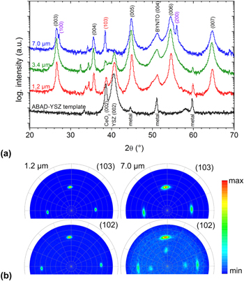
Figure 1. Phase purity and texture quality of BYNTO-doped YBCO layers of different thickness, (a) XRD θ-2θ scans, (b) XRD pole figures of the YBCO layer for two different films. The additional poles at Ψ ∼ 33° in the (102) pole figure of the 7.0 μm thick film arise from the a-axis-aligned texture component.
Download figure:
Standard image High-resolution imagePole figure measurements confirmed the epitaxial growth of the YBCO layer on the metal-based template as shown for two samples in figure 1(b). The in-plane FWHM values are about 8° for both BYNTO-doped and BHO-doped films. These values are slightly higher compared to undoped films (showing a typical FWHM <6° [5]) and remain almost unchanged up to a thickness of about 4 μm. However, the in-plane distribution gets significantly broader with further thickness increase and reaches a value of about 13° for the 7 μm BYNTO-doped film (see upper right pole figure in figure 1(b)). The larger in-plane spread might be correlated to the appearance of additional texture components observed by XRD. The in-plane FWHM values for the BYNTO (220) planes show the same trend (pole figures not shown). Furthermore, the YBCO (102) pole figure gives a clear indication for the a-axis-oriented texture component by the appearance of the additional spot at ψ ∼ 33°.
Figure 2 compares the surface morphology and cross-section of thick YBCO films for selected samples. The undoped film with a thickness of about 4.2 μm shows a high number of pinholes at the surface, which decouple the individual YBCO grains. Additionally, a high density of misoriented grains is visible at the film surface. A BHO-doped film of similar thickness shows a smaller number of misoriented grains and a significant reduction of pores. The denser microstructure is also verified in the cross-sectional view (inset of figure 2(b)). This is a striking contrast to the undoped film having the same thickness, where deep pores, large Y2O3 precipitates (white spots) and misoriented regions are visible in the upper part of the film (compare inset of figure 2(a)). One reason for the denser structure might be a refinement of the Y2O3 nanoparticles by the secondary phase additions, which results in a lower probability for the nucleation of misoriented grains. BYNTO-doped films with a thickness of more than 4 μm also show a dense YBCO matrix, but larger misoriented clusters on the surface are clearly visible in figure 2(c). A FIB cut of such a region, as shown in the inset of this figure, reveals that some grains are aligned perpendicular to the substrate surface as expected for a preferentially grown a-axis component. Other grains are tilted and might be connected to the (103)-textured YBCO component visible in the θ-2θ scans. So far it is not clear what causes the nucleation of these large clusters in thick BYNTO-doped films.
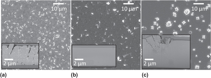
Figure 2. SEM images showing the surface morphology of (a) a 4.2 μm thick undoped, (b) a 4.4 μm thick BHO-doped and (c) a 7 μm thick BYNTO-doped YBCO film, respectively. Misoriented YBCO grains can be found in all films with a thickness above ∼4 μm. Insets: cross-sections of the samples showing pores for undoped YBCO, a dense microstructure for the 4.4 μm BHO-doped, and misoriented grains for the 7 μm BYNTO-doped YBCO film.
Download figure:
Standard image High-resolution imageFigures 3 and 4 give exemplary TEM images for thick BHO-doped YBCO layers and BYNTO-doped YBCO layers, respectively. The doping with BHO results in extended nanorods with an alignment almost parallel to cYBCO having an orientation spread to the substrate normal. The main component of the ensemble in figure 3(b) has an average tilt of 11° with a splay of ±3°, where occasional nanocolumns are within 4° of the c-axis direction. As shown before, the BHO nanocolumns are usually not perfectly straight but show a certain direction distribution along the length depending on the deposition conditions [16]. Additionally, there is a significant number of in-plane defects aligned in the (a–b)YBCO direction as small plates or stacking faults (figure 3(b)). The in-plane TEM view (figure 3(c)) indicates a diameter of about 4.6 ± 0.8 nm and a high areal density of 3040 μm−2 of these nanocolums, which corresponds to a matching field of 6.0 T. In some areas, a slightly lower nanocolumn density is observed, however also with matching fields around 5 T. The nanocolumns show a large splay of up to 20° ('fan-like structure') with occassional slight tilt of the main direction with respect to the substrate normal, figure 3(b).
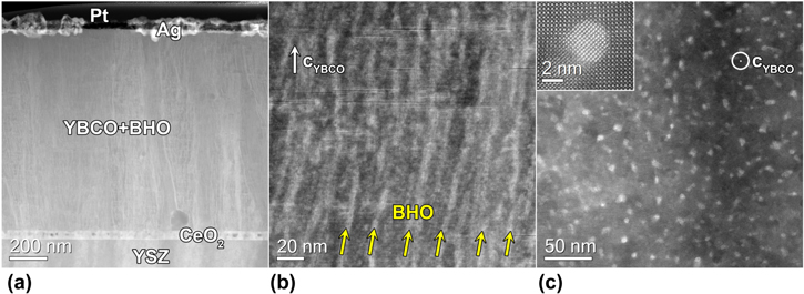
Figure 3. ADF-STEM images of a 1.2 μm thick BHO-doped YBCO nanocomposite on ABAD-YSZ tape in (a), (b) cross-section-view showing a large number of BHO nanocolums (some of them are marked by yellow arrows) aligned nearly parallel to the YBCO c-axis and (a–b)-aligned defects; and (c) top-view, white spots are the cross-sections of the BHO nanorods, the inset shows a high resolution image of one nanocolumn.
Download figure:
Standard image High-resolution image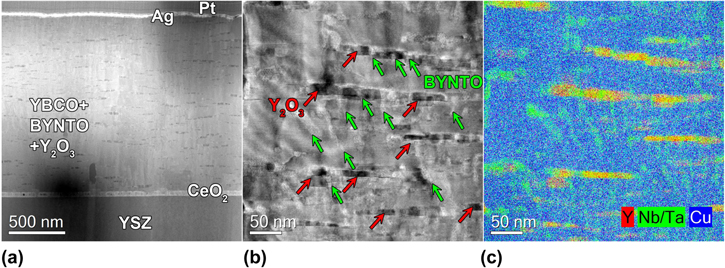
Figure 4. YBCO-BYNTO nanocomposite on ABAD-YSZ tape: HAADF-STEM (a) overview and (b) higher magnification image, showing the Y2O3 platelets (dark contrast features marked by red arrows) decorated by BYNTO (bright contrast features, some of them are marked by green arrows), with according (c) STEM-EDX Y–Nb/Ta–Cu composite map (Cu is shown in blue, Nb/Ta in green and Y in red).
Download figure:
Standard image High-resolution imageIn contrast, a more step-like pattern of cYBCO-parallel nanorods and (a–b)YBCO-oriented platelets is clearly visible for the BYNTO-doped film (figure 4). Whereas the fine nanorods with a diameter of about 7 nm show a pure BYNTO composition, the larger platelets of length up to 200 nm contain a significant amount of yttrium. A detailed analysis showed mainly pure Y2O3 platelets decorated with BYNTO particles. These individual platelets are biaxially oriented and grow parallel to the (a–b)-planes. However, ensembles of these platelets tend to have a certain angle (between ±4° and ±10°, figure 4) to the (a–b)-planes of the YBCO matrix due to a terrace-like configuration, as seen in figure 4(b). Such a microstructure of terrace-like 'composite defects' has been observed also in MOCVD-grown coated conductors [28], where an IBAD-MgO template was used showing an additional tilt of the matrix crystal structure [29]. However, no clear indication for a similar tilt of the YBCO matrix structure was found for the ABAD-YSZ templates used in this study. Finally, the few c-axis-oriented BYNTO nanorods have an areal density of around 1500 μm−2, corresponding to a matching field of around 3.1 T. An overview on the dependence of the nanoparticle distribution on the deposition condition can be found in our previous publication [16].
The resistively measured transition temperatures of Tc,0 = 89.3 ± 0.3 K (BYNTO-doped) and Tc,0 = 88.0 ± 0.4 K (BHO-doped YBCO), remain almost constant up to a thickness of 7 μm and are only slightly lower than the values of undoped films. In general, a constant Jc value (as obtained by scanning Hall probe microscopy) of about 0.6 MA cm−2 was determined for BHO-doped films with a thickness of 1–5 μm resulting in an Ic/w value of more than 300 A cm−1 (figure 5(a)). These Jc values are significantly lower compared to the undoped film, where a drop from 2.5 to 1.5 MA cm−2 was observed for the same thickness region [5]. The lower Jc values might partially originate from the lower Tc values; however, other effects as an insufficient oxygeneation or a different strain state due to the denser microstructure can not be excluded. Nevertheless, the Ic/w values are increasing almost linearly until a thickness of 5 μm in contrast to the undoped films, where no significant further increase was found above 3 μm [5]. Furthermore, the BHO-doped YBCO layers revealed a homogeneous Jc distribution in scanning Hall probe microscopy in liquid nitrogen temperature as shown for the 5 μm thick film (inset in figure 5(a)).

Figure 5. (a) Thickness dependence of Jc and Ic/w at 77 K for BHO-doped YBCO films, inset: Hall scan (4 mm × 5 mm) for the 5 μm thick film; (b) current density maps at 77 K for BYNTO-doped YBCO films having a thickness of 1.2 μm, 3.9 μm and 7.0 μm, respectively.
Download figure:
Standard image High-resolution imageThe BYNTO-doped YBCO films show a slightly different behavior. In this case, Jc values of about 1 MA cm−2 and 0.8 MA cm−2 were determined for the 1.2 μm and 3.9 μm thick film, respectively (figure 5(b)). The Jc distribution remains homogeneous; however, some regions with lower values are visible. Nevertheless, the resulting Ic/w value of 310 A cm−1 for the 3.9 μm thick film is even higher than for the BHO-doped sample with the same thickness. However, Jc of thicker films drops significantly to a value of about 0.3 MA cm−2 for 7 μm. This reduction is most probably correlated with the microstructural changes described before.
In summary, the incorporation of BHO or BYNTO secondary phase particles in the YBCO matrix leads to a denser microstructure and enables a preferential c-axis-oriented growth of the superconductor up to a thickness of more than 4 μm. This value is significantly higher than the typically reported values, showing the potential for a further improvement in Ic. Above 4 μm, more and more a-axis-aligned and misoriented grains result in lower Jc values. Possibly, this critical thickness for the nucleation of misoriented YBCO grains can be shifted to even higher values by careful adjustment of the deposition parameters.
3.2. Influence of the dopant on the Jc anisotropy
Three different films, i.e. pure YBCO, BHO-doped YBCO, and BYNTO-doped YBCO, with a thickness of about 1.3 μm were deposited on 20 mm long ABAD-YSZ templates to study the influence of the dopant on the microstructure and the anisotropy in more detail. The deposition conditions were further optimized to achieve an homogeneous film thickness on the longer substrates. All samples showed a homogeneous microstructure with a purely c-axis-oriented growth. The nanoparticles incorporated are biaxially oriented as discussed in section 3.1 and shown in [16].
All three samples reveal a homogeneous Jc distribution with some smaller defect areas, as checked by scanning Hall probe microscopy (figure 6). The average Jc value at 77 K in self-field reaches 2.2 MA cm−2 for the undoped film, whereas 0.9 MA cm−2 and 1.8 MA cm−2 were determined for the BHO- and the BYNTO-doped YBCO layer, respectively. The reduced Jc value for the BHO-doped film might be mainly due to the smaller Tc of about 87 K measured inductively for this sample in comparison to 89 K for the undoped and 90 K for the BYNTO-doped film, respectively. A similar trend for BHO-doped films was already found in previous studies, e.g. [30].
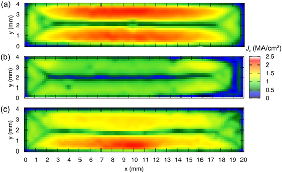
Figure 6. Critical current density maps of 20 mm long YBCO samples with a thickness of about 1.3 μm calculated from an inverted Hall scan at 77 K: (a) pure YBCO; (b) BHO-doped YBCO; (c) BYNTO-doped YBCO. The low Jc part in the central line and the diagonal features at the ends are geometric effects not related to the materials properties.
Download figure:
Standard image High-resolution imageSelf-field Jc values at 77 K of 3.6 MA cm−2, 1.6 MA cm−2 and 2.1 MA cm−2 for the undoped, BHO-doped and BYNTO-doped YBCO layer, respectively, were determined with transport measurements on microbridges. These values are slightly higher than the integral values calculated from the scanning Hall probe microscopy measurements, which originate both from the different electric field in the two types of measurements as well as from local variations of Jc.
The Jc(B, θ) anisotropy, θ being the angle between B and (a–b)YBCO-planes, for different temperatures and magnetic fields shows distinct differences between the different dopings, as summarized in figure 7 for selected datasets. The undoped YBCO film (red) shows high Jc values for fields parallel to the (a–b)-planes (θ = 90° and 270°) and a small peak for B∣∣c. The latter is related to aligned growth defects as for example grain boundaries originating from the granularity of the ABAD-YSZ template. In addition to the intrinsic electronic anisotropy, which accounts for a Jc anisotropy JcB∣∣(a−b)/JcB∣∣c of around 2 at 2 T, 77 K if only small, uncorrelated pinning centers were present (and hence a Jc of ∼0.3 MA cm−2 for B∣∣(a–b), stacking faults as well as (a–b)-aligned Y2O3 particles lead to a significant pinning contribution for B∣∣(a–b).

Figure 7. Comparison of the Jc anisotropy for different temperatures and fields for undoped (red), BHO-doped (green) and BYNTO-doped (blue) YBCO films grown on ABAD-YSZ templates.
Download figure:
Standard image High-resolution image
The BHO-doped sample (green) reveals smaller Jc values at 77 K due to the smaller Tc value. However, a strong peak for B∣∣c is visible at 2 and 5 T for both temperatures. This peak is shifted to higher angles due to the tilted orientation of the BHO nanocolumns. The shift of the (a–b)-peak to lower angles at low applied fields (where the direction of the applied magnetic field and the average vortex direction are not necessarily parallel anymore because of energy minimization [31]) has the same origin. The reason is mainly an increased pinning probability in the directions of smaller angles between the two sets of defect structures, c-axis columns and (a–b)-planar defects, called mixed pinning [32]. Apparently, the Jc values for B∣∣c at 64 K are significantly higher than for B∣∣(a–b). In general, BHO tends to form extended nanocolumns having some spread as shown in more detail in our previous publications (see figure 7 in [5]). These nanocolums have typical diameters of about 4 nm and are densely arranged in the YBCO matrix. Therefore, these nanocolums are strong pinning centers for B∣∣c in particular at lower temperatures (i.e. 40 K [5]).
The Jc(θ) curves of the BYNTO-doped films show a significantly reduced anisotropy. At 2 T, the BYNTO-doped film outperformes the undoped YBCO film for most field directions except near B∣∣(a–b). Additionally, a broad peak for B∣∣c is visible. This behavior results from the typical distribution of artificial pinning centers with short c-axis-aligned BYNTO nanocolumns and additional (a–b)-oriented BYNTO or Y2O3 platelets. At a closer look, both main directions, B∣∣(a–b) and B∣∣c, show a double peak structure at low magnetic fields (2 T) and more so at lower temperatures. This is explained by the effectively tilted defect microstructure of more or less well oriented short defects and the different elasticities of the vortices and hence trapping lengths in the (a–b)-planar defects. At high magnetic fields close to the (a–b)-direction, the flux lines follow the macroscopic direction of the applied field and align with the (a–b)-defects for B∣∣(a–b), which leads to a single peak at B∣∣(a–b). At low fields, they can be trapped by the individual defects and gain the largest energy now for fields applied parallel to the macroscopic direction of the defect structure, which leads to a double peak around 90°. The peaks are positioned at around ± 8°, which is comparable to the average angle of the platelets of 4°–10° from TEM, figure 4. Similarly, a broad double peak around 0° is observed at 2 T, 65 K, whereas at high fields, which exceed the matching field of the nanorod segments, no c-axis peak is visible. Similar double peak structures have been observed recently for (a–b)-planar SrTiO3 structures by Crisan et al [33] and for c-axis-oriented BaZrO3 nanorod segments by Malmivirta et al [34].
The technologically interesting minimum value of Jc for a certain field and temperature,  is slightly decreased by the BHO addition, but significantly increased for the BYNTO addition with respect to the pure sample at 2 T. This is a direct consequence of the complex pinning landscape with c-axis nanorod segements and (a–b)-planar platelet structures in the latter samples. At 5 T,
  is nearly the same in all three samples.
4. Summary
It was shown that doping of YBCO with either BHO or BYNTO nanoscaled secondary phase particle generates significantly denser microstructures and shifts the formation of misoriented grains to a higher film thickness compared to pure YBCO films. This leads to an almost linear increase of Ic/w for thicker films, as Jc stays almost constant above an initial decrease up to a thickness of more than 4 μm. For thicker films, an increasing amount of misaligned grains is observed leading to a limitation of the Ic/w values to about 300 A cm−1-w (77 K). Although the Jc values at 77 K are higher for undoped films, the performance of the doped films is superior in a wide angular range for higher magnetic fields as well as in reduced temperatures. This behavior originates in the case of BHO doping from the incorporation of c-axis-aligned nanorods resulting in a prominent c-axis peak in the Jc(θ) dependence. In contrast, BYNTO-doped samples show typically a mixture of short c-axis-aligned nanorods and (a–b)-aligned platelets leading to a flat Jc anisotropy. Therefore, the targeted incorporation of artificial pinning centers allows tuning the Jc anisotropy for specific applications.
Acknowledgments
The authors acknowledge financial support from EUROTAPES, a collaborative project funded by the European Union's Seventh Framework Programme (FP7/2007–2013) under Grant Agreement no. 280432. We thank A Usoskin (Bruker HTS GmbH, Germany) for the provision of buffered templates, and M Bianchetti, A Kursumovic and J L MacManus-Driscoll (University of Cambridge, UK) for the supply of BYNTO targets. The authors also gratefully acknowledge the technical assistance of J Scheiter, M Kühnel, U Besold (IFW) and R Nast (KIT).