

Abstract
In this paper, we show that the apparent delocalization of the conduction band reported from first-principles simulations for the high-mobility amorphous oxide semiconductor  (a-IGZO) is an artifact induced by the periodic conditions imposed to the model. Given a sufficiently large unit-cell dimension (over 40 Å), the conduction band becomes localized. Such a model size is up to four times the size of commonly used models for the study of a-IGZO. This finding challenges the analyses done so far on the nature of the defects and on the interpretation of numerous electrical measurements. In particular, we re-interpret the meaning of the computed effective mass reported so far in literature. Our finding also applies to materials such as SiZnSnO, ZnSnO, InZnSnO, In2O3 or InAlZnO4 whose models have been reported to display a fully delocalized conduction band in the amorphous phase.
Export citation and abstract BibTeX RIS
1. Introduction
Simulating amorphous structures from first-principles is a challenging task due to the aperiodic nature of the disordered phase. In crystalline materials, a structural model can be faithfully represented by a determined number of atoms packed in a unit cell periodically repeated, in which symmetries can be advantageously exploited. However, in amorphous phases its disordered nature prevents the use of symmetry and periodic operations. Further, the structural model being not well-defined, the development of reliable and predictable models is difficult. As a result, simulations of amorphous phases are often done using a pseudo-crystal approximation for which a 'large' unit-cell is used. It is then typically assumed that if the dimensions of the unit-cell are sufficiently large, the properties of the material are accurately captured.
This approach is conceptually similar to the so-called super-cell model typically used to study defects in crystalline materials [1, 2]. In this case, a sufficiently large super-cell ensures that no interaction occurs between the defects in periodic images, hence allowing a proper description of isolated defects. The adequate size of the model can then be assessed by establishing the convergence of the defect formation energy in the function of the model size [3]. Unfortunately for amorphous structures, there are no well-defined parameters to establish a similar approach. Hence, the number of atoms used in the model is mostly set by looking at the best trade-off between the computational resources required and the reproduction of experimental structural data such as bond lengths and atomic coordination numbers.
In this article, we focus on amorphous indium-gallium-zinc-oxide (a-IGZO) and show that the previously discussed approach is improper. Our findings are, however, not limited to a-IGZO but also extend to any material showing a delocalized band in its amorphous phase such as SiZnSnO [4], ZnSnO [5], InZnSnO [6],  [7] or
  [8].
[8].
A-IGZO is an n-type transparent semiconductor with particularly good mobility in its amorphous phase (>10  ) [9, 10] when compared to the common amorphous silicon (mobility <1
  ). These materials are relevant for thin film transistor (TFT) applications, typically used in display backplanes.
Most of the atomistic modeling studies reported so far for this material have opted for the use of a periodic model with a disordered structure with 84 atoms [11–16]. A surprising conclusion of these models is the sizable dispersion of the first unoccupied states as illustrated in figure 1. This dispersion suggests a strong delocalization of the corresponding wave-function. It is also possible to extract an apparent effective mass of ∼0.3me for this band, which actually matches the experimentally reported one ranging from 0.3me to 0.37me [13, 17–20].
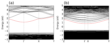
Figure 1. Pseudo-band structure of a-IGZO models. (a) For a quasi-cubic model with 105 atoms, (b) an elongated model with Lx = 57.7 Å, containing 350 atoms. The Fermi energy sets the zero. The first unoccupied band is colored in red. While all the bands are flat, the first conduction bands show an non-negligible dispersion indicating a strong delocalization of these states. In the case of an elongated model (panel (b)), the lower unoccupied state in the elongated direction (x,  -X in reciprocal space), the band flattens, indicating that the state has become localized. Subsequent unoccupied states can nevertheless still have a non-negligible dispersion (band width).
Download figure:
Standard image High-resolution imageTo provide a better understanding of this phenomenon, we study the variation of the conduction band delocalization with respect to the size of the model and show that this delocalization remains almost insensitive to the model dimensions until a threshold of ∼40 Å is reached. As from this point on, the states adopt a strongly localized character. The origin and the implications of this observation are analyzed.
2. Method
The simulations were performed within the density functional theory (DFT) framework. We studied 25 atomistic models of a-IGZO created independently using either a molecular dynamics approach through a melt and quenching method as detailed in [17] or through a seed coordinate-anneal algorithm proposed in [21]. The structures, lattice dimensions, number of atoms and method used to create each model are provided in the supplementary material (stacks.iop.org/JPhysCM/29/255702/mmedia). All models were relaxed with the CP2K package [22] using the PBE exchange-correlation functional [23] combined with a double zeta polarized basis [24]. The 25 models can be classified in two categories based on the shape of their unit cell, with either a quasi-cubic ( and
and  ) or an elongated parallelepiped one (
 and
and  ). The origin of the distorted cells arises from the unconstrained cell-relaxation applied to optimize the density of the models. For all cells, the length of the longest edge is labeled Lx.
For the quasi-cubic models, the number of atoms increases as a cubic function of Lx, leading quickly to simulations computationally intractable. Elongated cells, in contrast, lead to a linear increase of the number of atoms as a function of Lx, enabling the study of larger dimensions, while maintaining the computational effort accessible. Quasi-cubic models possess a number of atoms ranging from 14 to 315 for unit cell dimensions (Lx) going from 6.3 Å to 15.9 Å, while the quasi-parallelepiped ones increase from 161 to 350 atoms as Lx increases from 20.0 Å to 69.8 Å. The longest model is illustrated in figure 4. In order to evaluate how the delocalization of the wave function varies within models of a similar size, we use ten quasi-cubic models with a fixed number of atoms (105). Due to the nature of the disordered structure, the  value associated with these models varies between 10.9 Å and 11.2 Å. The distribution of the bond lengths and coordination numbers for the different models is provided in the supplementary material (figure S1).
Band structures and effective masses were obtained with the OpenMX code after atomic relaxation of the structure. For the metals, a simple s1p1d1 basis was used while for the oxygen site a more complete s2p2d1 basis was used. The simple s1p1d1 basis for the metal was found to be sufficient for an accurate description of the conduction band and allows for a substantial reduction of the computational cost for the largest structures (see supplementary figure 2 for a comparison of the pseudo band structure obtained with this basis set and with a 2s, 2p, 2d, 1f one for the metals). In order to improve the description of the electronic properties, a Hubbard correction term was included in the resolution of the Kohn–Sham equation with a U value of 6.08 eV [17].
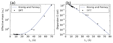
Figure 2. Variation of the conduction band (lower unoccupied state) effective mass in  (a) and of the conduction band dispersion (b) as a function of model length (Lx). The black stars represent the values extracted from DFT, the blue curves show the results obtained with a Kronig–Penney model as described in the text with an electron effective mass
  , a barrier width b = 0.8Lx and a barrier height
  eV.
eV.
Download figure:
Standard image High-resolution image3. Results and discussion
For models whose dimensions are smaller than 40 Å, the a-IGZO structures show a strong delocalization of the conduction band as illustrated in figure 1. The existence of this delocalized band allows the extraction of an effective mass (m*). The evolution of this effective mass at the bottom of the conduction band (in  ) in function of Lx, is plotted in figure 2(a). For Lx smaller than ≃30 Å, m* remains quasi unchanged and the resulting average effective mass is
  . For larger values of Lx, m* increases exponentially (figure 2(a)), which indicates that the conduction band wave-function becomes localized.
Interestingly, the constant value of m* for models with small Lx indicates that the form of the conduction band is only marginally altered in  when the model dimensions change. Another quantity of interest is captured by the band energy dispersion (or band width) defined as the change in energy between the center of the Brillouin zone (
 ) and its edge (X) located along the longest model edge (x).
As shown in figure 2, the effective mass tends to infinity and the dispersion is found to saturate towards zero upon the increase of Lx. These observations are in fact consistent with the expectations for an amorphous model. Indeed, a small effective mass and a large dispersion indicate the existence of translation symmetries in the material. Given that, by definition, amorphous materials have no symmetries, a large effective mass and a close-to-zero dispersion are hence expected.
The wave-functions extracted from the first conduction bands are sinusoidal and they are well fitted by a simple textbook model of a charge in an infinite well [25] as presented in figures 3 and 4 for the model with the longest unit cell ( ). A general solution of the Schrödinger equation for such an infinite well, in one dimension, is given by equation 1, where A is a normalization factor, n is a quantum number, x the position in the box and Lx the width of the well. Given this formulation, a fit of the DFT results can be used to extract the width of the well. Applied to the first eight wave-functions of the conduction bands in figure 3, the fit leads to an average width of the well of ∼40 Å. Given that the wave-function starts showing a localized character for a model for
  , the fitted well width provides a good indication of the minimum (Lx) required to induce a localization of the conduction band states.
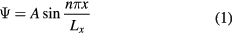
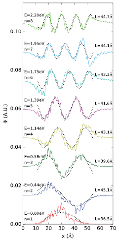
Figure 3. Projection in one dimension of the real part of the eight first conduction band wave-functions of the largest model (Lx = 71 Å) in real space. The wave-functions are taken in  . The projection is obtained by averaging the wave-function in real space in the y and z directions for any given x (which is the elongated direction, see figure 4(d) for conventions). The wave-functions are shifted with respect to each other for clarity, without the shift, all of the wave-functions fluctuate around zero. The shifts between the wave-functions are not proportional to their difference in energy. The latter, referenced as from the conduction band minimum, are provided on the left of the curves together with their associated quantum number n (see equation 1). The dotted black lines represent the expected form of the wave-function for a simple particle in a box in one dimension. The length of the box needed to reproduce the oscillation (Lx) is obtained by fitting and is listed as the inset on the right of the curves for each of the states. The representation of the four first wave-functions is illustrated in three dimensions in figure 4.
Download figure:
Standard image High-resolution image
Figure 4. Visualization in three dimensions of the real part of the four first conduction band wave-functions in  for the largest model (Lx = 71 Å) in real space. The color (blue/yellow) represents the sign of the wave-function. (a) Wave-function at the bottom of the conduction band, (b) second, (c) third and (d) fourth unoccupied state wave-functions.
Download figure:
Standard image High-resolution imageGiven the periodic boundary conditions used in our DFT simulations, it is more accurate to consider the wells as being periodic. Such a model, known as an electron in a Kronig–Penney potential [26], is often used to explain the appearance of band gaps in solid state physics textbooks [27]. This model has the advantage of degenerating to a single well model for sufficiently large barriers, allowing us to recover the results described previously while offering more insights into the interaction between the periodic images.
A schematic example of the Kronig–Penney potential is provided in figure 5. The model is characterized by five parameters: the effective mass of the electrons in the material (m*), the energies at the bottom of the well (V0) and at the top of the well (V1), the periodicity (Lx) and the barrier width (b). For simplicity, we assume that V0 = 0 and only consider the relative barrier height V ( ). The analytic solution of the Schrödinger equation for such a potential is described in [26, 27]. Note that two different effective masses can be defined, one in the absence of the Kronig–Penney potential, which is taken as a parameter of the model as described above, and a second one resulting from the presence of this potential, which modulates the effective mass introduced as a parameter.

Figure 5. Kronig–Penney potential. The energy at the bottom of the well is V0 and V1 at the top of the well. The periodicity is Lx and the barrier width is b.
Download figure:
Standard image High-resolution imageIn first approximation we use a barrier width linearly dependent on the periodicity. As discussed previously, it is expected that the Kronig–Penney model degenerates into the single well model for large values of Lx. From the material point of view, this is equivalent to considering that the spatial delocalization of the wavefunction becomes independent of Lx when Lx becomes large enough. As the width of this well (Lx − b) is expected to saturate for large periodicity Lx, the barrier width (b) must depend on Lx. While the linear dependence does not strictly fulfill these criteria, it is found to be sufficient to obtain a decent fit of the DFT results and allows the number of fitting parameters to be kept to a minimum.
Given the right set of parameters, the periodic model is able to fit well with both the modulation of the effective mass and the variation of the dispersion computed in DFT, as illustrated in figure 2. The values extracted from a fitting of the DFT results on this Kronig–Penney model should however be interpreted with care as many different sets of parameters allow for a good fit of the DFT results. This freedom in the choice of the fitting parameters originates mostly from the fact that the impact of a reasonable variation in one of the parameters can be compensated by a variation of other parameters as shown in figure 6.

Figure 6. Sensitivity of the variation of the dispersion with the model size for the Kronig–Penney model. Sensibility to (a) the effective mass, (b) the barrier height, (c) the barrier width. A lower dispersion indicates that an electron in a lower energy state would get confined between two barriers. If not provided in the legend, an effective mass  , a barrier width b = 0.8Lx and a barrier height
  eV is assumed.
Download figure:
Standard image High-resolution image
It is important to highlight that the results discussed in figures 2 and 6 correspond to the first unoccupied state in the DFT model and to the first allowed state in the Kronig–Penney model. While these states are localized in the largest models, higher energy states can nevertheless still be delocalized, as shown in figure 1(b), where the bands above the two first unoccupied bands start adopting sizable dispersion in the  -X direction. The Kronig–Penney model provides a straightforward explanation for this: the higher a state is in the periodic well, the more delocalized this state becomes. This is understandable as the effective barrier height experienced by the state decreases for higher-lying states. Nevertheless, as the energy of these higher-lying states decreases with the periodicity, they will eventually localize for sufficiently large periodicity.
Due to the exceptionally large delocalization of the conduction band, which we find to be of the order of 40 Å, periodic models with unit cells smaller than the delocalization length erroneously show that the conduction bands are delocalized over the complete material. This effect is nicely illustrated in figure 4 where the wave-function of the four first conduction bands are plotted for the largest model (Lx = 71 Å). In the x direction, along the longest edge, the wave-function displays the behavior of a simple particle in a well, as described above and in figure 3. In the two other directions, for which the width of the cell is much smaller than 40 Å, the conduction band remains fully delocalized and the effective masses in these directions adopt the expected value of 0.3me. This is also visible in figure 1(b); the first unoccupied states are well localized in the reciprocal direction  -X, but remain unchanged in the two other directions. These results imply that wave-function in the conduction band is, in good approximation, separable into three independent one-dimensional wave-functions for each of the reciprocal directions as proposed in [26].
The effective mass computed for the small models ( 0.3me) is surprisingly close to the values obtained experimentally ranging from 0.3me to 0.37me [20, 28] and the crystalline phase one (0.28me) [17]. This remarkable matching with the experimental measurements is unexpected as the computed value arises from an artifact induced by the periodicity imposed on the model. We argue in what follows that, even if this effective mass arises from an unrealistic periodicity, it still provides relevant information for the conduction mechanism.
The effective mass computed for the smallest models is a direct measure of the spatial delocalization of these wave-functions from which the conduction depends. This relation is visible in figure 6(a) which shows that the Lx required to localize the wave-function decreases with the effective mass used in the model. In other words, small effective masses lead to more delocalized wave-functions.
Conduction in a-IGZO is usually described by a phenomenological percolation model [29, 30]. The idea is that electron conduction in a-IGZO occurs in a similar way as in a normal crystalline material, through band-like transport, but in the presence of barriers for the conduction [29] or through a variation of the mobility edge in space [30]. Both models lead to the percolation of electrons through the material that limits, and explains, the conduction mechanism observed experimentally.
From a more fundamental point of view, we must account for the fact that the conduction band states are localized in space, as shown by the DFT calculations. Given this localized character of the electronic states, many other similar states must exist at different spatial locations within the material and these states must have very similar energies. Electrons can therefore jump from one state to another with a probability that depends on how close the states are distributed in space and energy. The conduction therefore depends on the hopping probability as well as on the number of hops needed to travel a certain distance. Hence, a large spatial extension of the states favors the conduction as less hops between states are needed to cover the same distance.
Interestingly, the mean free path of the electrons in the material is considered to be of a few nm [31] and is therefore of the same order of magnitude as the computed width of the delocalization of the wave-function. As most of the scattering mechanisms relevant for the conduction are inelastic, electrons are scattered into different energy states after each collision. This mechanism therefore enhances the probability of hopping from one state to another, increasing the conductivity. As the scattering mechanisms are temperature dependent, this idea is consistent with experiments showing that conductivity increases with the temperature [30].
In the models with small-scale periodicity, an interaction between the states in each periodic image is strictly imposed, leading to the perception of a delocalized band. This can be interpreted as if all the barriers between the lower energy states were eliminated. Such a model is inaccurate, which is why the effect of the barriers between the states needs to be re-introduced by invoking energy barriers in the conduction band to correctly describe the conduction mechanism. Models with small Lx in other words require an ad-hoc formalism to correctly describe the conduction mechanism. Provided such a correction, the effective mass extracted from these simulations gives meaningful information on how good the transport is in the material.
As we must conclude from properly-sized models, the conduction band of a-IGZO is constituted of localized states. The results reported so far in literature [11, 12, 14–16, 32] based on models of a-IGZO of modest dimensions should therefore be interpreted carefully. This is particularly true when they are used to analyze donor defects, such as oxygen vacancies, which interact with the conduction band. For these models, the conduction bands wave-functions appear to be independent of the position within the a-IGZO model. This is however not true for larger models where the wave-function is localized and hence has a clear maximum. Hence the behavior of the defects may depend upon its distance with respect to the localization centers of the conduction band state. Alternatively, the conduction band states themselves could be altered by the presence of the defect.
In the presence of charged defects, the cost in energy to add or remove an electron in the conduction band may also be affected. Indeed, the energy difference between the two first conduction bands, in  , decreases from 3.7 eV to 0.34 eV. Therefore, the energetic cost to add an electron to the second conduction band state (in
  ) gets much lower in a large unit cell model than in a smaller one. This can significantly modify the energetic behavior of the defects. It is important to note that this variation of the energy gap between the two first conduction bands is only indirectly linked to the number of atoms in the model. For instance, a quasi-cubic unit cell model, with 315 atoms (Lx = 15.9 Å), shows a
  eV while the elongated one, with 294 atoms (Lx = 38.8 Å), has a
  eV.
eV.
4. Conclusion
A-IGZO shows an uncommonly high delocalization of its conduction band states. The wave-function is found to be delocalized on up to ∼40 Å. Periodic simulation with unit cells smaller than the delocalization length led to an apparent wave-function delocalization over the complete material. Nevertheless, the effective mass extracted from these models is consistent with experimental results. This is explained by the fact that the forced periodicity eliminates barriers between the localized states, resulting in the computation of an apparent effective mass.
It is shown that the appearance of full band delocalization in amorphous models is an artifact resulting from the model size. The apparent delocalization gradually vanishes with increasing unit cell size for unit cells larger than the delocalization length of these states. The localization can be modeled with a Kronig–Penney model, which perfectly reproduces the apparent delocalization and small effective mass of periodically repeated small unit cells. For some materials, such as a-IGZO, the required simulation cell to fully localize the conduction states are computationally very demanding. However it was shown that the use of an elongated cell partially overcomes the problem as long as we consider properties in the elongated direction.
Finally, we rationalize the empirical electron transport model in a-IGZO, in which percolation barriers [23, 24] are invoked in an otherwise delocalized band. Indeed, we show that these percolation barriers apply the corrections needed to account for the localization of the conduction band states.
In the models used in the literature to study defects so far [11, 12, 14–16, 32, 33], the localization of the conduction band has not been accounted for. This implies that some of the conclusions drawn regarding the impact of these defects on the conduction and the electronic behavior of the material may have to be revisited.