
Abstract
In the present work, kelvin probe force microscopy (KPFM) technique has been used to study the CZTSe/CuxSe bilayer interface prepared by multi-step deposition and selenization process of metal precursors. Transmission electron microscopy (TEM) confirmed the bilayer configuration of the CZTSe/CuxSe sample. Two configuration modes (surface mode and junction mode) in KPFM have been employed in order to measure the junction voltage under illumination conditions. The results show that CZTSe/CuxSe has small junction voltage of ∼21 mV and the presence of CuxSe secondary phase in the CZTSe grain boundaries changes the workfunction of the local grain boundaries region. The negligible photovoltage difference between grain and grain boundaries in photovoltage image indicates that CuxSe phase deteriorates the higher photovoltage at grain boundaries normally observed in CZTSe based device. These results can be important for understanding the role of secondary phases in CZTSe based junction devices.
Export citation and abstract BibTeX RIS

Original content from this work may be used under the terms of the Creative Commons Attribution 4.0 licence. Any further distribution of this work must maintain attribution to the author(s) and the title of the work, journal citation and DOI.
1. Introduction
Cu2ZnSnSe4 (CZTSe) is a potential absorber material for solar cell applications [1–5]. A slight deviation from the optimal growth conditions of the kesterite phase result in the evolution of several secondary phases, such as ZnS, Cu2SnS3, SnS and CuS [6, 7]. Cu2ZnSnSe4 (CZTSe) thin films synthesized by different methods like stacked deposited precursors followed by selenization [8], microwave assisted chemical synthesis [9], solvent-thermal reflux method, [10] and magnetron sputtering of multilayers [11] all have the CuxSe secondary phase, even when the composition of the overall absorber layer is stoichiometric. In the reaction sequence of CZTSe, the elemental metals (Cu, Zn, Sn and Se) first form CuSe and then Cu2SnSe3, which forms the Cu2ZnSnSe4 phase on reaction with ZnSe. At high temperature (>500 °C), the CuxSe phase is formed due to a significant loss of SnSe2 [12]. The interfacial secondary phases in CZTSe based solar cell devices result in a high series resistance and can act as charge blocking layers [13]. The presence of secondary phases creates a discrepancy between the starting overall composition and the composition of the final CZTSe phase [14]. The phase inhomogeneity creates band gap fluctuations across the absorber layer and thus affects the performance of the device [15, 16]. The interface defects usually act as recombination centers in the space charge region, which reduce the open circuit voltage (VOC) and fill factor (FF) of the CZTSe/CdS device and therefore lead to low efficiency [17]. Secondary phases (e.g. CuxSe, ZnSe) may also be present in the form of nanoscale features between CZTSe grains [18, 19]. The highest efficiency (>20%) for Cu(InGa)Se2 (CIGS) is attributed to the grain boundary structure of CIGS having a Cu-poor structure, which acts as a potential barrier for holes and attracts minority carrier electrons, thus making carrier separation faster [1, 20]. This local built-in potential on grain boundaries was investigated by scanning kelvin probe microscopy [21]. CZTS was found to have a grain boundary structure similar to that of CIGS, thus the band bending at CZTS(Se) grain boundaries relative to intra-grain should lead to a solar cell conversion efficiency close to that of CIGS [20–22]. The presence of secondary phases on the grain boundaries can deteriorate this benign character of grain boundaries in CZTSe, and needs to be investigated. Secondary phases growing preferentially along CZTSe grain boundaries may affect the electrical properties of the bulk and grain boundaries in different ways. However, the investigation of the interface between a secondary phase and CZTSe is a complicated task [23, 24]. In the present study, we investigate an intentionally formed CZTSe/CuxSe interface using nanoscale KPFM measurements and transmission electron microscopy. The KPFM technique works here as a potential measurement method in order to map the open circuit voltage directly at operating conditions within the material without full device processing [25]. None of the other measurements can directly map the photovoltage within the material except KPFM technique [25].
2. Experimental
Magnetron sputtering has been used to prepare CZTSe/CuxSe heterostructure sample. A CZTSe thin film was prepared by magnetron co-sputtering on Mo-coated glass substrates using the metal precursors Cu, Zn, and Sn (Atomic % ratio; Cu: Zn: Sn = 48: 17: 35), followed by a selenization process at ∼520 °C for 10 min in a graphite box containing the sample and Se powder. Pure kesterite CZTSe and CuxSe films were prepared separately to compare the optical and structural properties of kesterite and CuxSe. To make the single phase films, the precursors (stoichiometric metal precursors Cu, Zn and Sn (Cu/Sn ∼ 1.87, Zn/Sn ∼ 1.30, Cu/(Zn + Sn) ∼0.81) for CZTSe or Cu-metal for CuxSe) were deposited on Mo coated glass and bare glass substrates followed by a selenization process identical to that for the bilayer sample.
Further, the bilayer sample was prepared by using initial compositions in off-stoichiometric ratio. The starting Cu concentration in the CZT precursor thin film (figure 1(a)) was higher (Cu/(Zn + Sn) ∼ 0.92, Zn/Sn ∼ 0.48) than the stoichiometric compositions. The Cu-rich precursor thin film will form CuxSe secondary phase along with CZTSe in the sample upon selenization (figure 1(b)). The resulting CZTSe thin film is Zn-poor, therefore, to make the top CZTSe layer near stoichiometric, a thin layer of Zn (∼60 nm) was deposited on top of the layer (figure 1(c)), followed by a similar selenization process as described above. The structural and optical characterization of the CZTSe and CuxSe samples after selenization were carried out by x-ray diffraction, Raman and UV-visible spectroscopic techniques. The synthesized bilayer sample is supposed to have both CZTSe and CuxSe phase layers and was characterized using cross-sectional TEM investigation, KPFM surface potential and photovoltage measurements. Prior to the imaging of the samples, the average work function of the Pt/Ir tip was calibrated as being ∼5.3 eV using a highly ordered pyrolytic graphite (HOPG) sample with a known work function value. The AFM tip radius of curvature is around ∼20 nm. The specimen for TEM study was prepared by focused ion beam (FIB) milling, on a gold support. A 40–50 nm carbon layer was deposited on the surface of the thin film to enhance the conductivity of the sample for lamella preparation and protect the top surface. The TEM study was performed at a FEI Tecnai Osiris operated at 200 kV equipped with a Super-X detector.
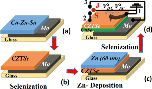
Figure 1. Schematic diagram illustrating the procedure adopted for synthesis of CZTSe/CuxSe bilayer sample [(a)–(c)] and the arrangement utilized for carrying out KPFM measurements in surface and junction mode [(d)].
Download figure:
Standard image High-resolution image3. Results and discussion
X-ray diffraction (XRD) patterns (figure 2(a)) and Raman spectra (figure 2(b)) of the CZTSe and Cu2−xSe thin film samples can be completely indexed as the pure phases (JCPDS no. 52-0868 and 34-171 were used as reference for the XRD peaks) [18, 19]. The UV-visible spectroscopic measurements show band gaps of 1.12 eV (CZTSe) and 1.72 eV (CuxSe) as specified in supplementary information is available online at stacks.iop.org/MRX/7/016418/mmedia. The effect of the CuxSe secondary phase on the physical properties of CZTSe based photovoltaic devices could be due to inhomogeneities in their band gaps as the band gap value is highly sensitive to structural disorder and deviations in stoichiometry. Therefore, the structure and composition of the bilayer film were characterized by transmission electron microscopy.
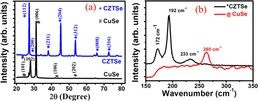
Figure 2. (a) XRD and (b) Raman spectra of stoichiometric CZTSe and CuxSe thin film samples.
Download figure:
Standard image High-resolution imageThe overview TEM image (figure 3) and STEM-EDX maps (figure 4) clearly show that the sample comprises of two different layers (labelled L1 and L2) along with a MoSe2/Mo substrate layer. Compared to the targeted Cu2ZnSnSe4 composition, layer L1 has a Zn-poor, Cu-rich stoichiometry (Cu: Zn: Sn: Se = 36.9: 2.3: 11.9: 48.9) and a thickness of 0.8–1.0 μm. Despite the deviating composition, the SAED pattern corresponds to a kesterite structure (figure 5). The Cu enrichment of this layer is presumably due to the presence of small particles, as seen in figure 5(c). These small particles are embedded in a Cu-rich layer which makes it difficult to confirm their Cu-rich nature. However, the same particles were observed in the Mo and MoSe2 layers, where we could determine their copper-rich nature (figure 6). Layer L2 has a thickness of 80–500 nm and consists of a homogeneous layer of SnO2 and Cu2−xSe (x  0) particles (Cu: Zn: Sn: Se: O = 43.8: 0.5: 15.4: 21.8: 17.6), which is confirmed by the ED ring pattern of this layer (figure 5). The MoSe2 and Mo substrate layers have thicknesses 100–340 nm and 330–400 nm, respectively. Layer L2 is firmly attached to L1 and no pores were seen at the interface between layers L1 and L2 (see supplementary information). The CuxSe phase exists as a buried phase in the active absorber layer CZTSe where the initial Cu-content might have influenced the formation of the secondary phase [26]. The presence of CuxSe phase in CZTSe thin film has also been reported in earlier studies [27].
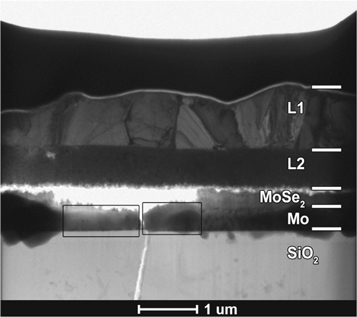
Figure 3. TEM overview of the cross-section lamella. The thickness of the thin film is ≈1.8–2.4 μm. L1 and L2 stand for Layer 1 and Layer 2, respectively. Rectangles indicate the amorphous parts of the Mo layer.
Download figure:
Standard image High-resolution image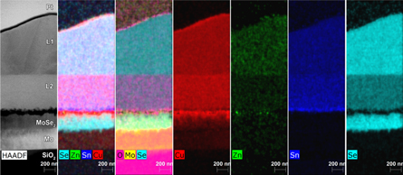
Figure 4. HAADF-STEM image, mixed ({Se, Zn, Sn, Cu}, {O, Mo, Se}) maps and individual element maps Cu/Zn/Sn/Se are shown in counts. The L1 layer contains Cu, Zn, Sn and Se, while L2 contains Cu, Sn, Se and O.
Download figure:
Standard image High-resolution image
Figure 5. Top: the TEM image of the two top layers is shown at the left. The right shows a HAADF-STEM image, where particles are observed in the L1 layer. Bottom: left shows the SAED pattern corresponding to one of the grains in L1. Right: for L2, the ring ED pattern can be indexed by the SnO2 and Cu2Se structures.
Download figure:
Standard image High-resolution image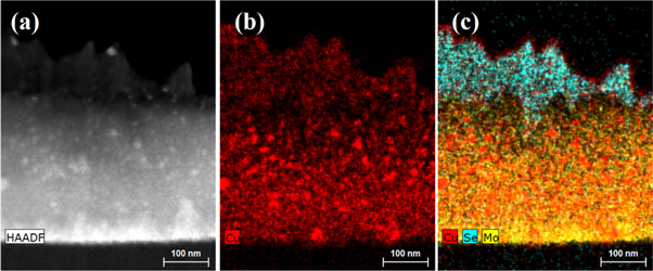
Figure 6. (a) HAADF-STEM image of the Mo and MoSe2 layers with the individual element map of (b) Cu and (c) the mixed {Cu, Se, Mo} map, given in counts. The observed particles are Cu-rich, which we assume to correspond to the observed particles in layer 1.
Download figure:
Standard image High-resolution imageFor the same bilayer thin film, the surface potential (SP) was measured in two modes: by applying AC-DC bias voltage between the top surface CZTSe layer and KPFM tip (surface-mode), or between the bottom layer (Mo) contact and KPFM tip (junction-mode). The grain boundaries in the kesterite acts as channel for carrier flow and these regions are dominated by thermally activated conduction mechanism [28–30]. The photovoltage at the interface was evaluated using point by point subtraction of the images obtained in the surface and junction modes under illuminated conditions. The work function of the top surface can be calculated by using equation  where ΦSample, Φtip and e are the work function of sample, tip, and electron charge, respectively. Initially, the SP of the CuxSe thin film was measured under dark condition. The SP image and corresponding work function histogram of CuxSe are shown in figures 7(b) and (c). Peak fitting in the SP histogram shows two peaks, one at 5.53 eV and a smaller peak at 5.50 eV, corresponding to grain and grain boundary (GB), respectively (figure 7(d)). In figure 7(d), line profiles along the height and SP images illustrate a lower work function at the GB (lower height) than at the grains (higher height) by about 30 meV and imply a downward band bending at GBs with respect to grains in the CuxSe layer. The morphology of the bilayer sample also confirms that the average grain size of CZTSe is in micron range (figure 7(e)). The SP variation of the CZTSe layer is shown in figure 7(g) in terms of work function and has been deconvoluted into two peaks (figures 7(f) and (g)). The line profile analysis of CZTSe along the grains and GBs establishes a higher work function at GBs in comparison to grains by about 50 meV, indicating upward band bending at GBs in the CZTSe layer. It is interesting to note that the band bending at GBs in CZTSe is opposite to that observed in the CuxSe layer.
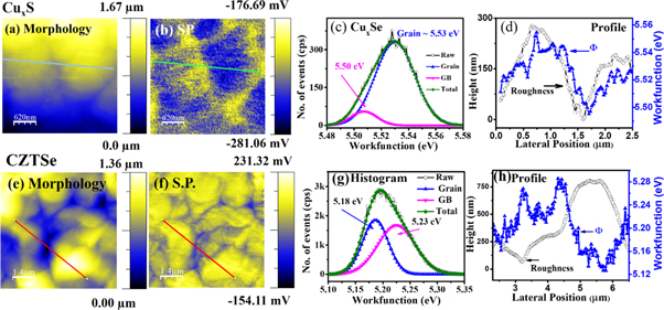
Figure 7. CuxSe: (a) Morphology, (b) Surface potential, (c). WF histogram and (d) Line profile of pristine CuxSe thin film. CZTSe: (e) Morphology, (b) Surface potential, (c) WF histogram and (d) Line profile of CZTSe thin film sample.
Download figure:
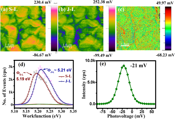
Standard image High-resolution imageThe effect of CuxSe on the CuxSe/CZTSe sample was further investigated by carrying out measurements in surface and junction modes under light conditions. The average SP (work function) of the bilayer in surface mode is ∼110 mV (Φ ∼ 5.19 eV), in junction mode ∼90 mV (Φ ∼ 5.21 eV). The photovoltage map of the CZTSe/CuxSe junction is obtained by subtraction of surface potential images corresponding to surface and junction modes under illumination, as shown in figure 8(e). The average photovoltage in the bilayer sample is ∼21 mV at the CZTSe/CuxSe interface. The photovoltage of the bilayer sample corresponds to the difference between the Fermi levels of the CZTSe and CuxSe thin films, i.e. quasi Fermi level under light conditions. The photovoltage histogram shows that the interface voltage is ∼21 mV at both grain and GB within the resolution limit of the KPFM. In an earlier study, it was shown that the presence of CZTSe/Secondary phases interfaces at the junction (CZTSe/CdS) region results in narrowing of the band gap at the interface side which means higher recombination at the interface as the energy barrier for recombination is reduced [31].
Figure 8. CZTSe/CuxSe : (a) SP image in S-L mode, (b) SP image in J-L mode, (c) Photovoltage map obtained by subtracting the SP images of S-L and J-L modes, (d) Workfunction histograms of SP images of S-L and J-L modes and (e) Histogram of photovoltage image.
Download figure:
Standard image High-resolution image
Earlier reports using KFPM two configuration method (surface and junction) on a CZTSe/CdS solar cells showed a higher photovoltage at the GB and this higher photovoltage was attributed to the GB of CZTSe [32]. But the presence of the CuxSe phase apparently reduces this feature as there was no significant difference between the photovoltages at grain and GB in the present study. This KPFM method also allows to record the interface voltage by measuring SP on the surface of CZTSe/CuxSe heterostructure sample. This shows that the presence of the CZTSe/CuxSe interface reduces the benign character of CZTSe GBs, which are generally considered to have a positive charge due to Cu+ vacancies. The interface voltage between CZTSe/CuxSe is found to be ≥ 21 eV, which can be responsible for the open circuit voltage deficit in the CZTSe based solar cell device. The suppression of grain boundaries feature in CZTSe thin film reduces the potential difference between grain and GB which will slow the charge carrier separation under illumination conditions. The higher the photovoltage between the CZTSe and CuxSe interface, the higher will be the VOC deficit in the CZTSe/CdS based photovoltaic device. CuxSe is found usually in CZTSe thin films due to Sn-loss during selenization which influences the Cu content, resulting in the formation of secondary phases. The impurity phase present on the top surface can be etched by a chemical process, but its presence across the cross-section can be a critical cause of a shunt path across the absorber of the CZTSe solar cell [18]. Improvement in the photovoltage directly depends on controlling the recombination in the GB of CZTSe and at the interfaces between CZTSe/secondary phases [27]. Since the GB barrier height is highly sensitive to Cu/[Zn + Sn], the performance of CZTSe solar cells can deteriorate because of the presence of secondary phases at the GB of the absorber layer [33]. Carrier separation at the GBs can be affected by the presence of CuxSe phase at the GB which can alter the surface charge and defects around the GB.
4. Conclusion
In conclusion, this study reports KPFM based investigation of a model CuxSe/CZTSe bilayer sample. The surface potential measurements in surface and junction modes indicates a photovoltage drop ≥ 21 mV at CZTSe/CuxSe interface. The presence of CuxSe secondary phase in CZTSe can potentially invert the band bending at G.B. of kesterite absorber. The similar photovoltage value at grain and grain boundaries in CuxSe/CZTSe is quite different to the higher photovoltage observed at grain boundaries observed normally in CZTSe/CdS solar cell device [29]. This results may represent the deteriorating effect of CuxSe secondary phase in CZTSe solar cell device having CuxSe phase.
Acknowledgments
Authors acknowledges support provided DST in the forms of InSOL and Indo-Swiss projects. We also acknowledge Joke Hadermann EMAT, University of Antwerp, Groenenborgerlaan 171, B-2020 Belgium for helping in TEM measurements. M V Manoj Vishwakarma acknowledges IIT Delhi for MHRD fellowship. Prof B R Mehta acknowledges the support of the Schlumberger chair professorship. M V also acknowledges the support of DST-FIST Raman facility.