

Abstract
Quantum phase slips represent a coherent mechanism to couple flux states of a superconducting loop. Since their first direct observation, there have been substantial developments in building charge-insensitive quantum phase-slip circuits. At the heart of these devices is a weak link, often a nanowire, interrupting a superconducting loop. Owing to the very small cross-sectional area of such a nanowire, quantum phase slip rates in the gigahertz range can be achieved. Instead, here we present the use of a bias voltage across a superconducting loop to electrostatically induce a weak link, thereby amplifying the rate of quantum phase slips without physically interrupting the loop. Our simulations reveal that the bias voltage modulates the free energy barrier between subsequent flux states in a very controllable fashion, providing a route towards a phase-slip flux qubit with a broadly tunable transition frequency.
Export citation and abstract BibTeX RIS
1. Introduction
The macroscopic quantum coherence of the superconducting wavefunction is accompanied by a plethora of consequent phenomena, among which is flux quantization. Due to the single-valuedness of the wavefunction, the magnetic flux enclosed by a superconducting loop must be quantized, hence the flux state of the loop is precisely characterized by the phase winding number n.
To make a transition between two flux states of a superconducting loop, the phase of the order parameter ψ must make a discontinuous jump by an integer multiple of 2π, referred to as a phase slip [1]. The phase discontinuity occurs locally at a point where the modulus  is strongly suppressed. These events can be broadly classified into deterministic and stochastic phase slips. Deterministic phase slips occur when the free-energy barrier to the subsequent flux state is reduced to zero by increasing the external magnetic flux [2, 3]. For a non-zero barrier, a stochastic phase slip, via either thermal activation over the barrier [3–5] or quantum tunneling [6–8], can occur, and its rate depends exponentially on the barrier height.
Tunneling through the free-energy barrier, referred to as quantum phase slips (QPS), explains the non-zero resistance of ultra-thin superconducting nanowires at very low temperatures [9]. In 2005, however, Mooij suggested that quantum phase slips can coherently couple the discrete flux states of an isolated superconducting loop, a phenomenon dubbed coherent quantum phase slips (CQPS). Consequently, he proposed that a charge-insensitive qubit can be constructed by embedding a nanowire in a superconducting loop, in a manner that it presents a weak link and becomes a favorable spot for nucleation of phase slips, and CQPS results in the superposition of two distinct macroscopic flux states [10, 11]. CQPS can be understood as a phenomenon dual to the Josephson effect, where coherent exchange of vortices along the phase-slip line plays the role of Cooper-pair tunneling across an insulating barrier [12–16]. Phase-slip flux qubits have been demonstrated using disordered superconducting nanowires [17–19]. Moreover, their experimental realization spurred interest in fabricating other quantum phase-slip circuits such as quantum interference devices [20, 21], and single-charge transistors [22, 23].
In this paper, we circumvent the need for advanced nanostructuring by controlling the weak links in a superconducting ring electronically. More specifically, we present in detail the effect of a bias voltage on quantum phase slips in continuous, uninterrupted superconducting rings. In particular, we characterize the free-energy barrier between flux states for various ring geometries as a function of bias voltage using the time-dependent Ginzburg–Landau (GL) simulations, and reveal that the barrier can be precisely tuned down to vanishingly small values, for which the rate of quantum phase slips is strongly amplified. As a consequence, such design can serve as a model for a phase-slip flux qubit whose transition frequency is electronically tunable in a broad frequency range.
This paper is organized as follows. First, a background on deterministic and stochastic phase slips is given in section 2. In section 3, the effect of bias voltage on the free-energy barrier between subsequent flux states is discussed in detail. Finally, in section 4, we present a model for an electronically-controlled phase-slip qubit, and discuss the achievable rate of quantum phase slips as a function of the bias voltage for various ring geometries. Section 5 summarizes our results.
2. Phase slips in a superconducting ring
Transitions between flux states of a superconducting loop occur via either deterministic or stochastic phase slips. For a deterministic phase slip to occur, the magnetic flux threading the loop must be increased till the free-energy barrier to the subsequent flux state is brought to zero. For a loop of radius R whose width and thickness are much shorter than the coherence length  and the penetration depth λ, the critical flux for a transition from the flux state n = 0 to n = 1 is given by [24–26]
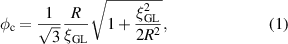
where the flux φ is normalized by the quantum of flux  . The critical flux defines the Eckhaus instability point where fluctuations of the order parameter, either due to noise or sample inhomogeneities, can grow to nucleate a phase-slip event [25]. For instance, the transition from n = 0 to n = 1 occurs at
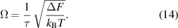
  , as illustrated in figure 1.
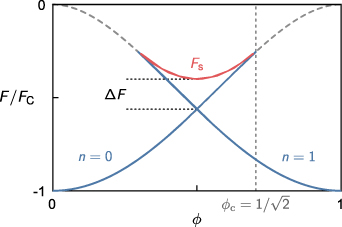
Figure 1. Free energy F of a superconducting loop of radius  , normalized by the condensation energy
  . The enclosed flux φ is normalized by the flux quantum Φ0 = h/(2e). The blue line is obtained from a numerical solution of the GL equation, where a deterministic transition from the flux states n = 0 to n = 1 occurs at
  . The grey dashed lines correspond to the free-energy in the absence of any fluctuations. The energy barrier ΔF is defined as the difference between the saddle state
  (red solid line) and the energy of the flux states.
Download figure:
Standard image High-resolution imageThe occurrence of a deterministic phase slip presumes flux can be increased till the instability point is reached. However, as the flux increases the energy barrier between flux states decreases, and a stochastic phase slip is more likely to occur. In other words, thermal activation over the barrier or macroscopic quantum tunneling, can result in a phase slip well before the instability point is reached.
Within the framework of the Langer–Ambegaokar–McCumber–Halperin (LAMH) theory [27, 28], the rate of thermally-activated phase slips (TAPS), is given by

where ΔF is the free-energy barrier, and the attempt frequency can be written as
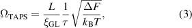
where L is the length of a wire or the circumference of a loop, and the relaxation time is defined as
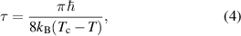
where  is the critical temperature of the superconductor. Analogously, the simplest form for the rate of quantum phase slips is obtained by replacing the thermal energy
  by ћ/τ, leading to the expression [29]

where a and B are numerical factors of order unity. This phenomenological model has been shown to fit the resistance of ultra-thin wires quite accurately [9, 30, 31].
The essential parameter in the rate expressions is the barrier ΔF, defined by the trajectory the loop traverses to make a transition between two metastable flux states [27]. These trajectories are characterized by intermediate saddle points in the free-energy landscape, referred to as saddle states. Based on LAMH theory, the energy barrier is defined as the difference between the free-energy of the saddle state  and the initial flux state (see figure 1).
For a loop with a circumference  , the free energy of the saddle state reads [32]
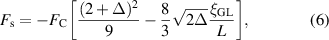
where  is the condensation energy, and Δ is a parameter denoting the difference between the maximum and the minimum of the order parameter of the saddle state, and can be determined from the transcendental equation [32]
as a function of the normalized flux φ.
The energy of the saddle state  , along with the barrier ΔF, is illustrated in figure 1. A distinction can be made between a stochastic phase slip occurring well before the instability point, and a deterministic one occurring at the critical flux
  . Evidently, the free energy barrier vanishes at the instability point.
In the limit  , and in the absence of external magnetic flux (i.e. φ = 0), the barrier reduces to the original formula obtained by the LAMH theory for a one-dimensional wire
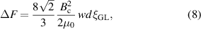
where  is the thermodynamic critical field, and the product wd is the cross-sectional area. The energy barrier is linearly proportional to the product of the cross-sectional area and the coherence length, which intuitively corresponds to the volume over which the modulus of the order parameter goes to zero to allow a phase discontinuity. Consequently, quantum phase slips are typically observed in superconducting wires that are only few nanometers in width[9, 17–19].
3. Transitions between flux states in the presence of bias voltage
To allow for less stringent requirements on the cross-sectional area of the superconductor, one must employ an additional barrier-reducing mechanism, thereby compensating for the increased area to preserve the rate of quantum phase slips. In this section, we show that bias voltage modulates the energy barrier, and subsequently the rate of stochastic phase slips. To visualize the effect of the bias voltage (see figure 2), we resort to the simulations based on the time-dependent GL equation [33, 34]
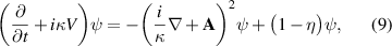
where V is the electrostatic potential, and  is the magnetic vector potential. The complex order parameter is defined as
  . Equation (9) is written in a dimensionless form where the space coordinate is scaled by the penetration depth λ and the order parameter by its equilibrium value [1], where κ stands for the
  ratio. The time t is scaled by the ratio
  where
where  is the diffusion coefficient.

Figure 2. Model for a superconducting ring of radius R and a width w, subjected to a bias voltage  . The angle between the bias contacts is denoted by α, whereas the extent of each contact is quantified by the angle γ.
Download figure:
Standard image High-resolution imageIn our simulations, equation (9) is solved self-consistently with the continuity equation, which in the Coulomb gauge reduces to
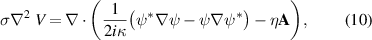
with the dimensionless conductivity σ given by  , where
  is the normal-state conductivity and µ is the magnetic permeability. The supercurrent stemming from the superconducting order parameter ψ for given magnetic field satisfies the Neumann boundary conditions at all sample boundaries, and the electrostatic potential is bound by the value of bias defined between the voltage leads.
3.1. Superconducting ring with a width 

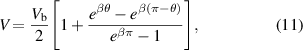
To gain an insight into the effect of bias voltage, we first consider a model where the ring width w is much shorter than the coherence length and the penetration depth  . As a consequence, the variation of the order parameter along the radial direction is negligible. Furthermore, we set the angle α = π, the potential
  , and V(0) = 0 (see figure 2).
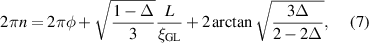
Due to the bias voltage, the order parameter exhibits a non-uniform profile along the circumference of the ring with minima at θ = π/2 and 3π/2, where θ is the azimuth angle (see figure 1 in the supplementary material (stacks.iop.org/SUST/33/125002/mmedia) for an example of the supercurrent density induced by bias voltage). These weak points serve as a preferential location to nucleate a phase slip. In particular, based on the summation of the current driven by bias voltage and the current driven by the external flux, the phase-slip location is determined. For instance, in the flux state n = 0, the minimum is at θ = π/2, whereas in n = 1 state it is at θ = 3π/2.
Importantly, because of this additional current induced by bias voltage, deterministic phase slips can occur at a lower magnetic flux. For instance, the critical flux, given in equation (1), for the transition from n = 0 to n = 1 decreases as a function of bias voltage, and tends to the degeneracy point φ = 1/2 (see figure 3(a)).

Figure 3. Effect of bias voltage on a superconducting loop. (a) The critical flux  as a function of bias voltage
  for various radii of the ring. The dots represent the simulated data points. (b, c) Comparison between analytical (solid lines) and numerical (crosses) solutions for the scalar potential V and the superfluid velocity
  as a function of the azimuth angle θ. Parameters used: κ = 1, σ = 1, and
  .
.
Download figure:
Standard image High-resolution imageFor a ring of a radius comparable to the coherence length, and in the limit of small bias voltage, we obtain an analytical solution for the scalar potential
and for the superfluid velocity
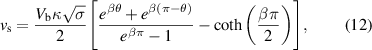
where  . These expressions agree well with the GL numerical solution, as depicted in figure 3(b,c). Evidently, the superfluid velocity at the phase-slip center (either at θ = π/2 or 3π/2) increases linearly with bias voltage, thereby reducing the magnetic flux required for a deterministic phase slip.
Equivalently, from the energy standpoint, as the bias voltage increases, the free-energy barrier between subsequent flux states decreases. Importantly, because the saddle-state energy is weakly dependent on flux near the degeneracy point φ = 1/2 (figure 1), the energy barrier between the states n = 0 and n = 1 can be conservatively approximated by

which can be extracted from the numerical solution of the GL equation (as depicted in figure 4(b)). This approximation is valid in the limit that the bias voltage is large enough to reduce the instability point to the vicinity of the degeneracy point.

Figure 4. Free-energy spectrum of a voltage-biased superconducting ring threaded by a solenoid field. The free energy is normalized by the condensation energy  , and the flux enclosed within the ring by the flux quantum. The unbiased case (
 ) is shown in (a), whereas a bias voltage
  is used for ((b)–(d)). The angle α between the bias contacts (see figure 2) is varied between the panels. A conservative estimate of the free-energy barrier ΔF, in line with equation (13), is depicted in (b). Parameters used:
  , κ = 1, γ = 7° and σ = 1.
Download figure:
Standard image High-resolution imageMoreover, because there is a single favourable location to nucleate a phase slip, the barrier is not reduced uniformly along the loop. Put differently, there is a single location in the ring where attempts to escape the present flux state go through a reduced barrier. For other locations, the barrier is effectively not reduced. To account for this non-uniformity, the ring can be divided into two sections, a section with a length  where the barrier is reduced due to the presence of bias voltage, and a section with a length
  where the barrier is effectively uninfluenced. The rate of phase slips occurring in the latter will be much lower than the former due to the exponential dependence of the rate on the barrier height. Therefore, in the presence of bias voltage, the attempt frequency must be modified to
3.2. Superconducting ring with a finite width
Before proceeding to evaluating the rate of quantum-phase slips, we examine the effect of bias voltage on a superconducting ring of finite width w. In contrast to the previous section, the magnetic flux now comes in two flavours, either as localized within the ring or uniform throughout the space.
First we consider the localized case, where the magnetic field is focused through e.g. solenoid core piercing the ring. The free-energy spectrum of the unbiased ring is shown in figure 4(a). Since the body of the superconducting ring is not exposed to any external magnetic field, all the minima of the free-energy are at integer flux quanta and have the same energy. Moreover, the degeneracy point between two flux states n and n + 1 is exactly at  , where φ is the normalized flux enclosed by the inner/outer rim of the ring.
In agreement with figure 2, upon biasing the superconducting ring, the critical flux for a deterministic phase-slip tends to the half-flux quantum. However, depending on the angle α between the contacts, one can selectively favor transitions that increment or decrement the vorticity of the ring. For instance, for α = 180°, the bias voltage divides the ring into two symmetric arms, thereby the summation of the current induced by bias voltage and the circulating current due to the enclosed flux is identical in the states nth and n + 1. Thus, the symmetry of the free energy spectrum is preserved, as seen in figure 4(b) (see also figure 2 in the supplementary material).
In contrast, for α = 120°, the current induced by the bias voltage in the upper shorter arm of the ring is larger than its counterpart in the longer arm. As a consequence, this geometry favors transitions that increment the vorticity of the ring (see the free energy spectrum in figure 4(c)). A mirror reflection of this energy spectrum is obtained for the explementary angle  , where vorticity-decrementing transitions are favored.
Second, we consider the case of a uniform magnetic field. The main difference with the solenoid case is that the vortex dynamics is no longer solely governed by the flux-quantization requirement, but also by the Meissner effect since the magnetic field impinging on the ring will be screened. Accordingly, as evident in figure 5(a), the minima of the free-energy deviate from the integer flux quantum. Moreover, in terms of the flux φ enclosed by the outer rim, the degeneracy point between flux states are at [35]
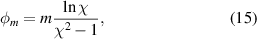
where m is an integer, and the ratio χ is defined as R/(R + w). Similar to the solenoid case, the bias voltage reduces the free-energy barrier, or equivalently the critical flux for a deterministic transition to the subsequent flux state. Incidentally, the uniform case tends to the solenoid case as the width of the ring decreases in comparison to the coherence length.

Figure 5. Free-energy spectrum of a voltage-biased superconducting ring in a uniform magnetic field. The free energy F, normalized by the condensation energy  , is given as a function of the external magnetic flux enclosed by the outer rim of both unbiased (a) and biased (b) rings. The dotted-grey lines represent the degeneracy points between flux states, as given in equation (15). Parameters used:
  , κ = 1, α = 180°, γ = 7°, and σ = 1.
Download figure:
Standard image High-resolution imageBased on figure 4 and figure 5, for a symmetric free-energy barrier between two flux states n and n + 1, the ring must be locally flux biased with  . Moreover, upon employing bias voltage to modulate the barrier, an angle α = π must be used if preservation of symmetry is needed.
4. Proposal for a phase-slip flux qubit
To tune the transition frequency of Josephson-based qubits, the junction must be replaced by two in parallel, thereby forming a SQUID. The effective Josephson energy of the SQUID—and in turn the transition frequency of the qubit—depends on the overall magnetic flux enclosed by the SQUID loop [36–38]. The additional flux-bias loop, however, renders Josephson-based qubits sensitive to flux noise, which motivates the need for establishing electronically tunable weak links. For example, references [39, 40] suggested placing the superconductor in a planar electric field to locally suppress the Cooper-pair density and hence form a weak link. In this paper, however, we suggest inducing the weak link in a superconducting ring using bias voltage. In this section, we calculate the free-energy barrier for voltage-biased aluminum nanorings and the corresponding rate of quantum phase slips. Moreover, we propose using these rings as phase-slip flux qubits, where the transition frequency is tunable by bias voltage.
The parameters for aluminum are in line with those measured in reference [31]. Specifically, the critical temperature  is 1.32 K. For our calculations, we assume
  , such that the rate of thermally-activated phase slips is suppressed, and quantum phase slips dominate. Although the time-dependent GL equations are derived in the immediate vicinity of the critical temperature, they have been extensively used in literature, and their predictions agree well with experiments even away from the critical temperature. In our approach, we follow the success of recent simulations in reference [41], using the same empirically introduced temperature-dependence of the superconducting length scales, beyond the GL theory as originally derived.
The bias voltage is applied along the outer rim of the ring, where the geometry is characterized by the angles α and γ, as depicted in figure 2. Since our purpose is to symmetrically couple the flux states n = 0 and n = 1, we take the angle α = π and the applied magnetic flux is localized within the ring throughout this section. We consider a superconducting ring of radius R = 100 nm, width w = 100 nm, and thickness d = 10 nm, and investigate how the critical flux changes as a function of the superconducting length-scales of the Cooper-pair condensate. Namely, motivated by the ever-present disorder in experimentally deposited samples, we vary the mean-free path  , which in the dirty limit changes the coherence length and the penetration depth of the ring. For each mean-free path, the normal-state resistivity is obtained from the well-known relation
  cm2 for aluminum thin films [42].
The critical flux  as a function of the bias voltage is shown in figure 6 for
  6, 9, and 12 nm. The corresponding coherence lengths at the considered temperature are
  , and 150 nm. Evidently, for less disorder, i.e. larger mean-free path, the coherence length increases. Accordingly, the ratio between the width of the ring and the coherence length decreases, thereby approaching the one-dimensional limit where
  . As a consequence, the critical flux at which a deterministic phase-slip occurs is reduced. Furthermore, in accordance with figure 3(a), as the radius of the ring increases with respect to the coherence length, the critical flux increases. In our subsequent analysis, we limit ourselves to one particular choice of the mean-free path, namely
  nm and detail the effects of geometry on performance of the proposed device.

Figure 6. Critical flux  for a deterministic phase-slip as a function of the bias voltage
  , for three aluminum rings with different mean-free paths
  . The radius of the rings is R = 100 nm, and their width w = 100 nm. Dots show the simulated data points.
Download figure:
Standard image High-resolution imageFirst, we explore the effect of the bias contact angle γ (see figure 2) on the relation between the energy barrier and the bias voltage. As expected, the energy barrier decreases as a result of increasing the bias voltage (as shown in figure 7(a)). More important, the descent rate, characterizing the effectiveness of bias voltage, also depends on the angle γ. As γ decreases, the slope decreases, denoting to a reduced sensitivity to bias voltage.

Figure 7. Quantum-phase-slip rate as a function of bias voltage  . (a) Free-energy barrier ΔF for a superconducting ring of radius R = 100 nm, width w = 50 nm, and thickness d = 10 nm for various bias contact angles γ (see figure 2). Dots show the simulated data points. (b) Free-energy barrier ΔF as a function of the ring width, for fixed γ = 18°. The dotted line corresponds to an angle γ = 13.5° for the case w = 100 nm, for comparison with the case of
 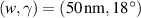 , having the same γ (R + w) product. (c) The rate of quantum phase slips
  corresponding to the panel (a). (d) Sensitivity of the largest quantum phase slip rates on the bias voltage, for three thicknesses of a disordered aluminum ring, namely d = 5, 10, and 15 nm (and remaining parameters
  nm, R = 100 nm, w = 50 nm, and γ = 3°).
Download figure:
Standard image High-resolution image
Second, we explore the effect of varying the width of the ring while keeping the bias angle γ = 18° unchanged (figure 7(b)). Evidently, the larger the width, the higher the energy barrier since the condensation energy of the ring increases, as given in equation (8). Thus, a larger bias voltage is required to reduce the barrier to zero. To decouple the effect of enlarging the ring from the increased arc length of the bias voltage contacts, we present the dotted line for w = 100 nm and γ = 13.5° in figure 7(b), having the same product γ (R + w) as the sample with w = 50 nm and γ = 18° (shown as blue curve in figure 7(b)). The direct comparison of the two cases for fixed γ (R + w) product reveals nearly identical slopes of their ΔF(w) characteristics. Incidentally, for precise control over the free-energy barrier, and subsequently the rate of stochastic phase slips, the width of the ring must be comparable or even smaller than the radius of the ring. This requirement ensures that the supercurrent induced by bias voltage flows predominantly azimuthally. Otherwise, the radial component of the current becomes important, and can strongly suppress the Cooper-pair density near the biasing leads, thereby changing the preferential location of phase-slips. A detailed discussion on the effects of ring size on the behaviour of the proposed device is provided in the supplementary material.
The corresponding rate of quantum phase slips is shown in Fig 7c, calculated based on equation (5), in the strong damping regime with 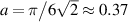 , as derived in reference [43]. With the bias voltage increased, the rate of quantum phase slips increases exponentially to the gigahertz regime, where a desired qubit level spacing is achieved. Specifically, at the degeneracy point φ = 1/2, the eigenstates of the ring are the symmetric and the anti-symmetric superpositions of the flux states n = 0 and n = 1. Incidentally, the superposition of two macroscopic flux states were first measured in references [44–46] for superconducting rings interrupted by one or more Josephson junctions.
The Hamiltonian of this two-level system takes the form

up to a constant energy shift corresponding to the operating point F(φ = 1/2). Based on figure 7(b), the operational bias voltage is determined by the width of the ring. Moreover, the tunability of the qubit is determined by the geometric extent of the bias voltage over the outer rim of the ring, characterized here by the biasing angle γ.
Various insights into the tunability/sensitivity of the proposed qubit as a function of the device geometry can be obtained by approximating the relation between the free-energy barrier and the bias voltage to be linear (see figure 7(a)). In particular, the rate of quantum based slips can be cast in the form
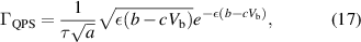
where the dimensionless constant  , b is the free-energy barrier, normalized by the condensation energy, at zero bias voltage, and c is the slope. Maximizing equation (17), the highest phase-slip rate is
  , at a bias voltage
 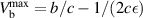 . Consequently, for a fixed frequency operation, it is preferential to operate at the sweet spot
  where the rate is insensitive to charge fluctuations in the first order. The tunability/sensitivity of the qubit can be characterized by the full width at half maximum (FWHM) given by
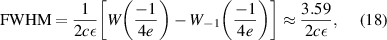
where W is the Lambert function. Consequently, to reduce the qubit sensitivity, the biasing angle γ must be minimized to reduce the slope c, along with reducing the the relaxation time τ and condensation energy, for instance by using a ring with a smaller thickness d, as depicted in figure 7(d).
To sum up, the bias-induced modulation of the energy barrier is a double-edged sword. On the one hand, it allows for tuning the transition frequency, a desired quality in qubits. On the other hand, due to the exponential dependence of the rate of quantum phase slips on the barrier, the qubit is sensitive to charge fluctuations. As seen in figure 7(d), bias voltage fluctuations in the order of 1 µV shift the qubit transition frequency by a few gigahertz.
The main advantage of the proposed qubit is that the rate of quantum phase slips, and in turn the transition frequency of the qubit, depends on macroscopic parameters, namely the geometry of the ring and the coherence length of the superconductor. As a consequence, it is immune to fluctuations and defects occurring over a length scale much shorter than the coherence length. Moreover, because the bias voltage provides a complete control over the free-energy barrier (figure 7), it can absorb small deviations of the superconducting parameters, thereby ensuring a well-defined transition frequency.
5. Summary
As the main topic of this paper, we have set out to investigate the effect of bias voltage on the transitions between subsequent flux states of a superconducting ring in an external magnetic field. Our time-dependent GL simulations revealed that the applied bias voltage suppresses superconductivity in the arms of the ring, thereby electronically inducing a weak link for nucleation of quantum phase slips. Moreover, the bias voltage controllably modulates the superconducting carrier density in those weak links, so that the free-energy barrier between flux states can be precisely tuned. That in turn governs the dynamics of deterministic and stochastic phase slips, where the rate of quantum phase slips increases exponentially as a function of bias voltage.
Based on the demonstrated barrier reduction by electronic means, we estimate the rate of quantum phase slips in typical aluminum nanorings to reside in the gigahertz range. This frequency is further tunable by sample size and width, quality of the material (i.e. mean-free path and the coherence length of the superconducting condensate), as well as by temperature. Our general findings are not sensitive to the imperfections in the sample geometry or position and size of the leads. Accordingly, our results suggest a roadmap towards the most broadly tunable phase-slip flux qubits to date, with rather robust operation and precise electronic control, and without need for challenging nanostructuring beyond the fabrication of the ring itself.