
Novel Reversible Comparator Design in Quantum Dot-Cellular Automata with Power Dissipation Analysis


1
Department of Electrical Engineering, Islamic Azad University of Science and Research Tehran (Kerman) Branch, Kerman 7718184483, Iran
2
Department of Mathematical Modeling, North-Caucasus Federal University, 355017 Stavropol, Russia
3
Department of Modular Computing and Artificial Intelligence, North-Caucasus Center for Mathematical Research, 355017 Stavropol, Russia
4
Department of Information and Communication Technology (ICT), Mawlana Bhashani Science and Technology University, Tangail 1902, Bangladesh
5
Facultad de Ingeniería y Ciencias, Universidad Adolfo Ibáñez, Diagonal Las Torres 2640, Peñalolén, Santiago 7941169, Chile
6
Waste Science & Technology, Luleå University of Technology, SE 971 87 Luleå, Sweden
7
RIKEN Center for Advanced Photonics, RIKEN, Wako 351-0198, Saitama, Japan
8
Department of Electrical and Computer Engineering, University of Saskatchewan, Saskatoon, SK S7N5A9, Canada
*
Author to whom correspondence should be addressed.
Appl. Sci. 2022, 12(15), 7846; https://doi.org/10.3390/app12157846
Submission received: 21 May 2022
/
Revised: 29 July 2022
/
Accepted: 2 August 2022
/
Published: 4 August 2022
(This article belongs to the Section Quantum Science and Technology)
Abstract
:In very large-scale integration (VLSI) circuits, a partial of energy lost leads to information loss in irreversible computing because, in conventional combinatorial circuits, each bit of information generates heat and power consumption, thus resulting in energy dissipation. When information is lost in conventional circuits, it will not be recoverable, as a result, the circuits are provided based on the reversible logic and according to reversible gates for data retrieval. Since comparators are one of the basic building blocks in digital logic design, in which they compare two numbers, the aim of this research is to design a 1-bit comparator building block based on reversible logic and implement it in the QCA with the minimum cell consumption, less occupied area, and lower latency, as well as to design it in a single layer. The proposed 1-bit reversible comparator is denser, cost-effective, and more efficient in quantum cost, power dissipation, and the main QCA parameters than that of previous works.
Keywords:
QCA; reversible logic; comparator; Feynman gate; TR gate; coplanar; quantum cost; energy dissipation1. Introduction
Many researchers today consider quantum cellular automata to be a foundation for quantum physics [1]. Reversible logic is used to realize quantum systems and circuits. With the advancement of technology in all fields of the electronics industry, especially in the design of digital circuits, energy and power consumption are of great importance. The power dissipation generated by conventional logic circuits can be remedied by reversible circuits [2]. The reversible logic is that the energy dissipation during a circuit can be reduced to zero if it is possible to go from the final states to the initial states, regardless of what happens along the way. In these circuits, one can stop at any stage of the path, return to the previous stages, and access the circuit inputs. In fact, in these circuits, there is a 1-to-1 relationship between input and output vectors. This means that, not only can the outputs be obtained by 1-to-1 correspondence of the inputs, but the outputs can also be obtained from each input [3,4]. Reversible logic circuits consist of a wide range of applications, including quantum computing. QCA is being evaluated as a novel technology that has excellent properties at the nanoscale [5,6]. This technology is different than conventional technology, and it does not use any current or voltage to transmit information. Rather, a coulombic relation the QCA cells created paths for propagation and the transmission of information; these paths are called QCA wires [7]. On the other hand, one of the basic blocks in digital logic design is comparators, which compare two numbers. The optimal, cost-effective, and efficient design of circuits and base blocks helps us achieve more efficient, cost-effective, and complex circuits. As a result, this paper provides an optimal layout of the 1-bit comparative building block by reversible logic and implementation in QCA as a single layer (coplanar) with minimum cell consumption, occupied area, and less latency. In this paper, we initially propose an improved QCA scheme from FG and TR gates. The optimal design of the reversible comparator is then obtained using these TR and Feynman gates. Then, the proposed design is compared with previous work. The article is further prepared into five parts. Section 2 provides the basic QCA terminology and an overview of basic QCA comparators. The design and implementation for the proposed circuits are presented in Section 3. Tables, graphs, and power dissipation analyses are presented for comparison with previous work in Section 4. Finally, the conclusions are presented in Section 5.
2. Background Materials
2.1. QCA Basic Terminology
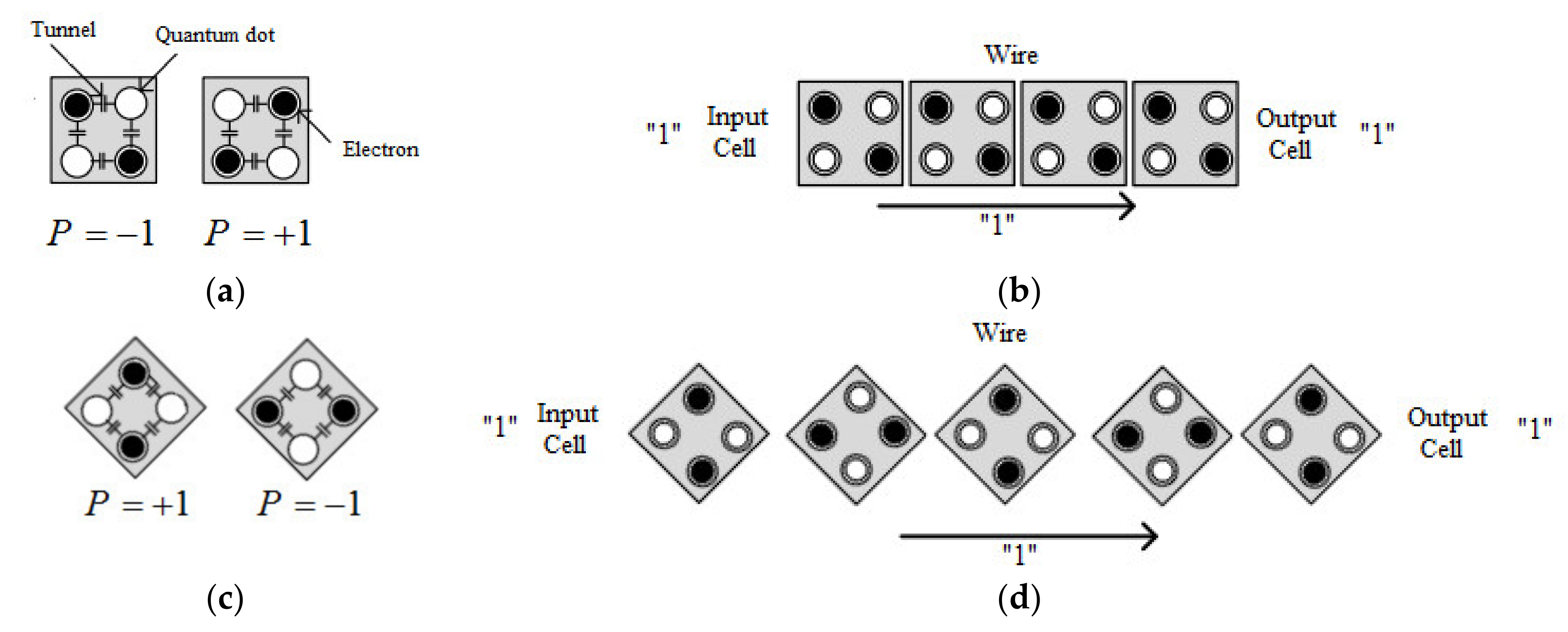
Circuits are designed and implemented in QCA, based on QCA cells. As mentioned in QCA technology, communication and calculations are achieved via the interaction of coulombic repulsion of QCA cells and influence on neighboring cells, in order to influence the electrons enclosed in each cell, thus transmitting and spreading information [7]. As a result, based on the interaction of coulombic repulsion, QCA wire is used for the communication required in QCA, and digital gates are used to create its computing circuits. Figure 1a shows the QCA 90-degree cell in both logical 0 and 1 modes [7,8,9,10]. Coulombic energy is used between neighboring cells for data transfer and QCA operations. QCA wire is created from an array of QCA cells and by stacking them together in such a way that, by entering an input with a logical value of “1” or “0”, from the input cell to the output cell, the polarization of the cells will be the same. The input will bring all the cells to their polarity. Figure 1b shows the QCA 90-degree wire used to propagate the signal [8,9].
Another type of coplanar wire is known as 45-degree wire. This wire is created by using a 45-degree cell and putting this type of cell together [7]. Figure 1c shows the QCA 45-degree cell. Figure 1d also shows the QCA 45-degree wire. As you can see, this type of QCA wire is created using 45-degree cells. In this type of wire, the values of the input logic are propagated in the odd cells, with the inverter the values of the input in the even cells. Since the 45-degree cells have less strength, due to the 45-degree rotation of the cell, the designs made with this type of cell have more implementation cost and less strength. Therefore, we have not used any 45-degree cells in our designs [7,8,9]. On the other hand, the QCA clock (Figure 2) was used to synchronize circuits [11,12]. QCA clock has four phases, which are required for control signals and circuit synchronization.
The confluence of two QCA wires is called a crossover. In order for QCA wires to not destroy each other’s data at the crossovers of two wires, QCA crossovers are used. There are two different types of crossovers in QCA. The first type is known as multilayer crossovers. As seen in Figure 3a, in this type, one of the wires is passed through the intersection in one layer (first layer), and the other wire is passed in the third layer, so that the wires keep their data and prevent data destruction. We have not used this type of crossover, due to the high cost of implementation and large occupied area and volume [13].
The second type of QCA crossover is referred to as coplanar crossover. This type of crossover is created in two ways. In the first method, the coplanar crossover, is created using both 45° and 90° wire types. Figure 3b shows this type of crossover. As you can see, in this method, one of the wires is a 90° wire (standard wire), and the other wire is a 45° wire. As explained, in the 45° wire, in order for the input data to be received in the output cell, the number of cells must be odd. As a result, in this method, the number of cells must be odd. We have not used this type of crossover either, as we said before, due to the use of a 45° cell [14].
Another method of coplanar crossover design is only achieved by using standard wire. In this method, both wires are created using 90-degree cells, and non-adjacent clock phases are used at the crossover, so that the wires do not destroy each other’s data. Figure 3c shows both types of QCA wire coplanar crossovers for coplanar designs. As you can see, in this method, one of the wires must be two clock phases ahead or two clock phases behind the other wire [15].
The 3-input majority gate (MV) is shown in Figure 4a, in which, by fixing one of the 3-input MV inputs and providing the logical value “0”, the AND gate is created; the OR gate is created by fixing one of the 3-input MV inputs and providing the logical value “1” [10,16]. Figure 4b,c shows the 2-input AND and OR gates. The inverter gate is also shown in Figure 4d.
2.2. Comparator
The comparator circuit is a combinatorial logic circuit to compare two numbers, which defines whether they are equal and which one is bigger or smaller than the other [17,18]. Table 1 is the truth table, and Figure 5 is the block diagram from this circuit. The output equations A > B, A < B, and A = B are as follows:
3. The Proposed Circuits
3.1. Reversible Comparator with QCA
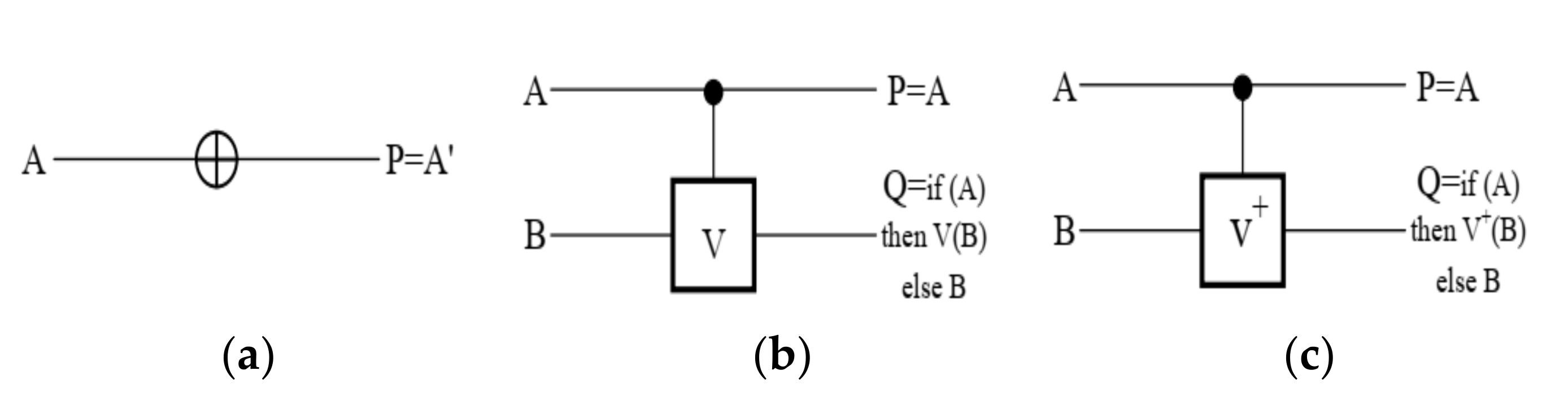
The reversible logic circuits have the unique outputs for each of the inputs, and each of the inputs for the reversible circuits can be estimated from their outputs. In reversible circuits, the number of inputs is equal to outputs [3,18,19]. Extensive articles on reversible comparators have been presented by many researchers. However, in this paper, we propose an optimal design of the reversible comparator relative to the circuit presented in [2], based on [20], and describes its QCA implementation. In the reference [2], a comparator design, based on TR and FG gates, is presented; it is a design with a quantum cost of 9, which is a lower quantum cost than similar works. Figure 6 shows the quantum implementations. As shown in the figure, the quantum implementation of the inverter in (a), the control V in (b), and (c) also represents the quantum implementation of V+.
3.2. Design of FG
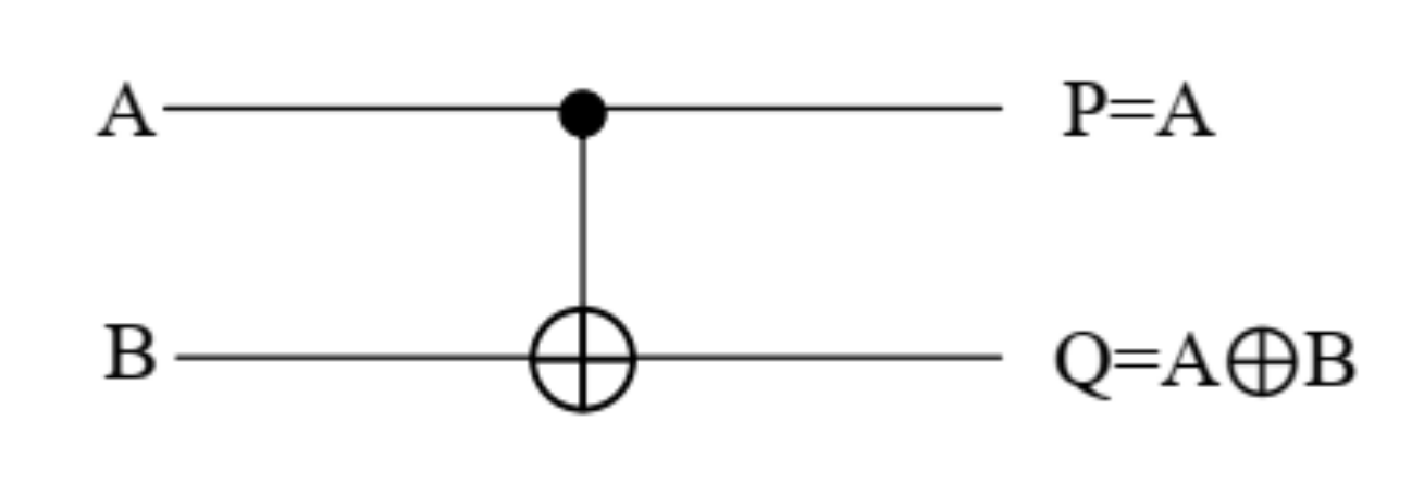
FG is one of the reversible gates that consists of two inputs and two outputs. A and B are the input bits; P and Q are also the outputs bits of this gate. Figure 7 shows the quantum implementation of this gate. The quantum cost of this gate is equal to 1 [20]. Table 2 also shows the truth table of this gate. The logical equations of the P and Q outputs are as follows:
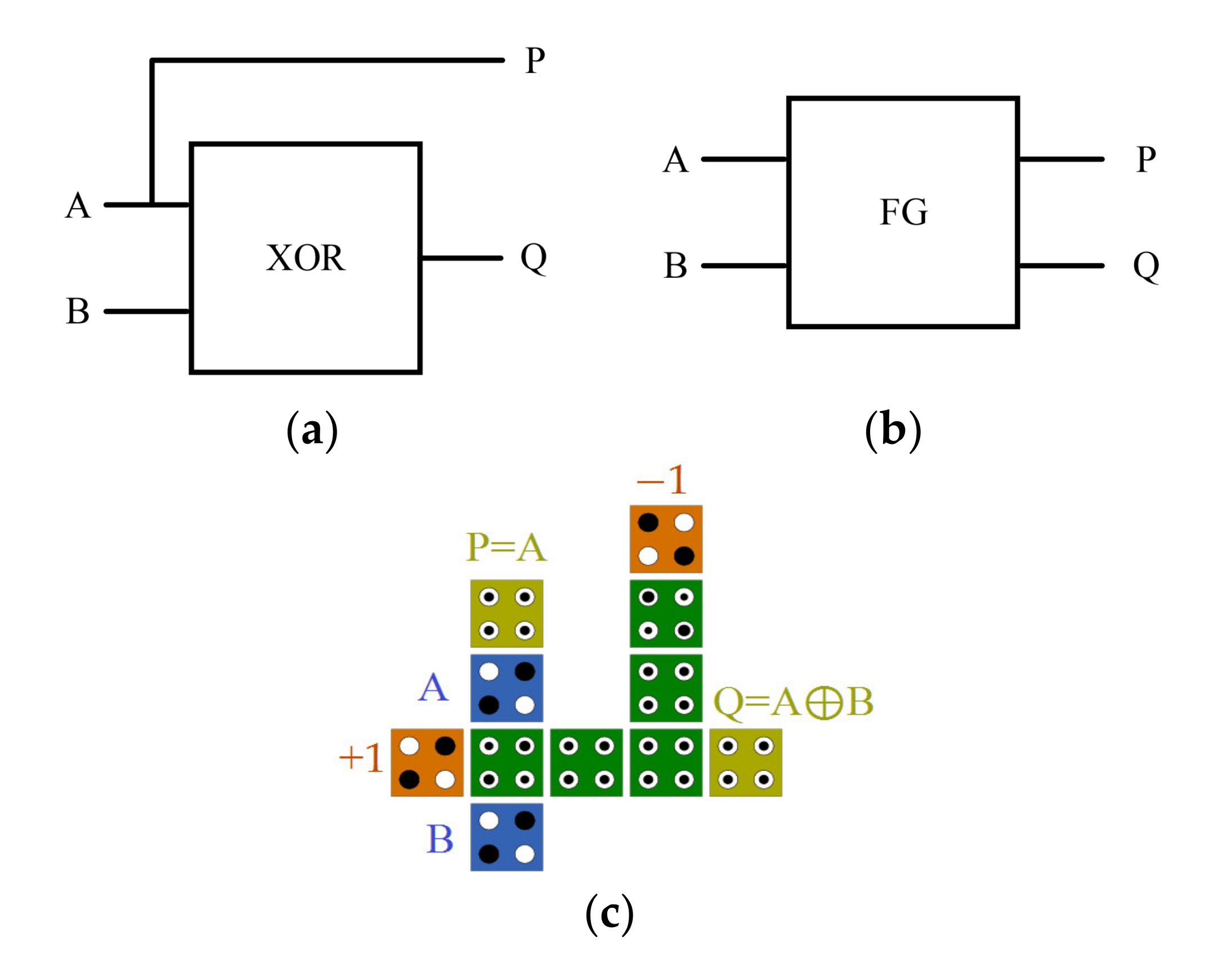
The logic and block diagram and QCA implementation for FG are represented in Figure 8.
3.3. Design of TR Gate
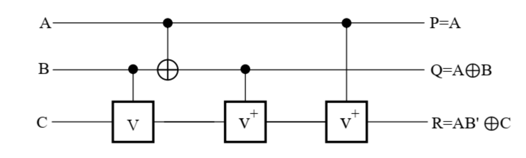
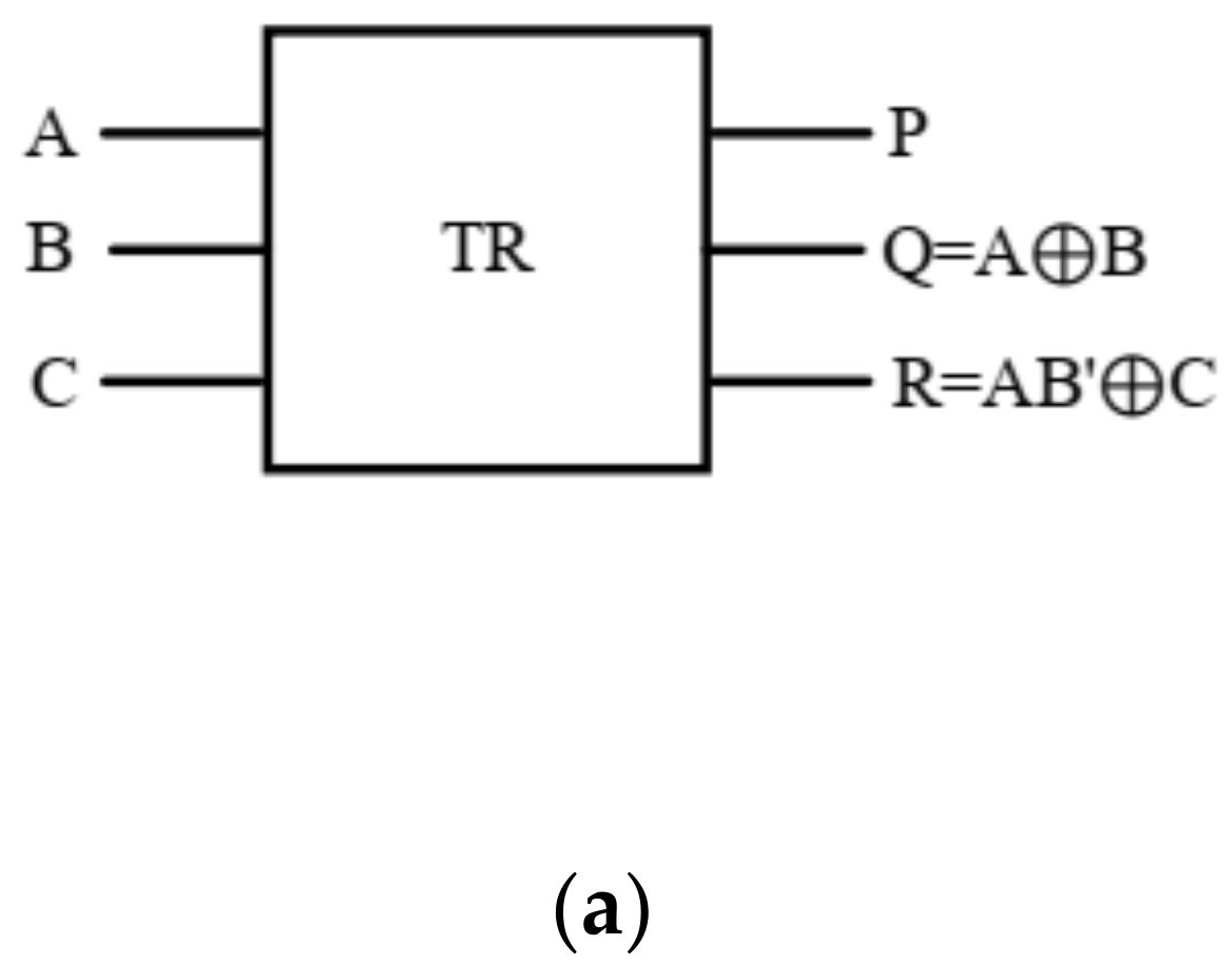
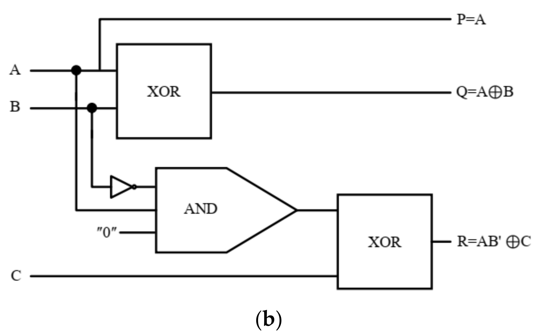
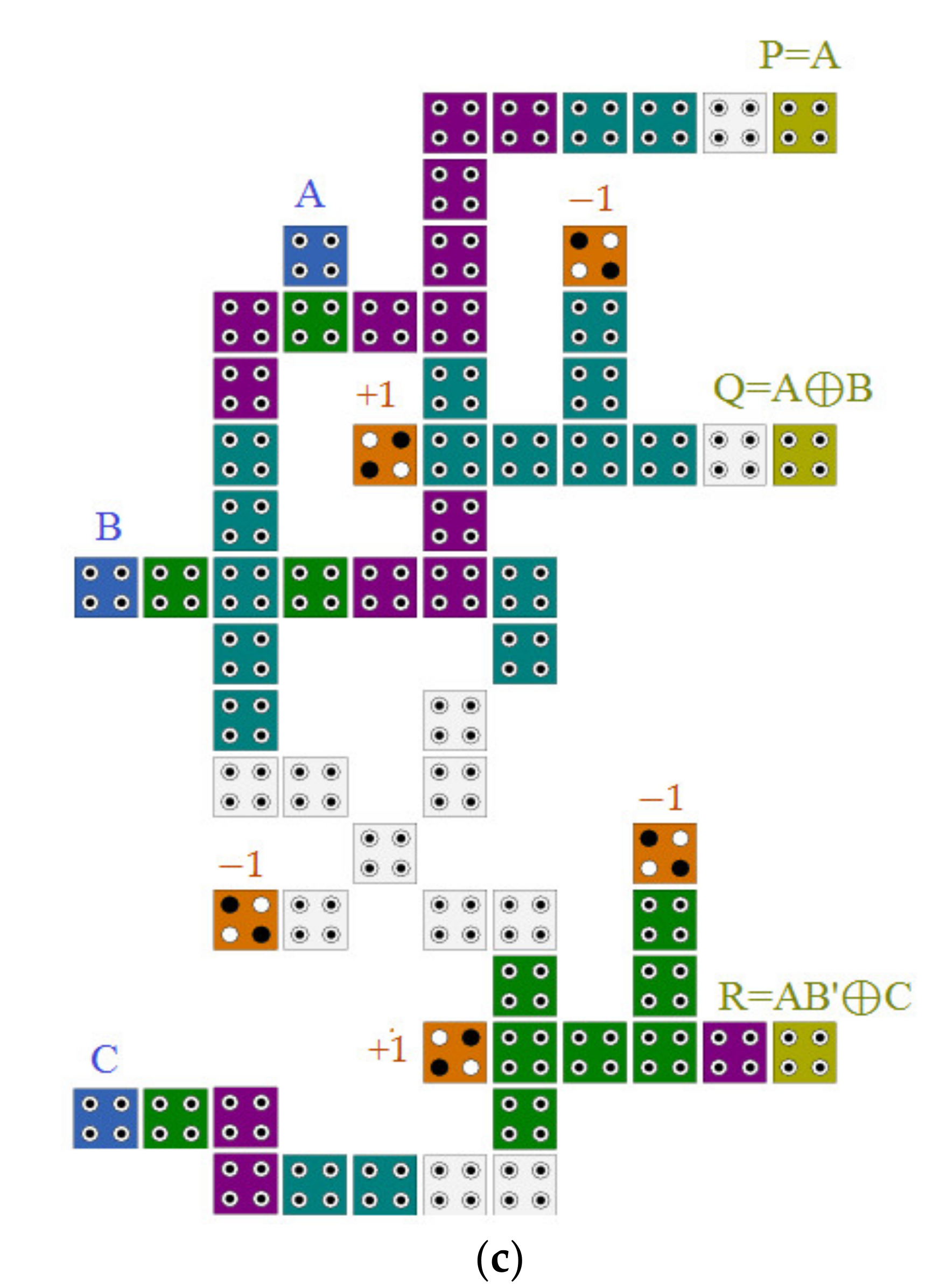
The TR gate is another reversible gate consisting of three corresponding unique inputs and outputs [21]. Figure 9 shows the quantum implementation from this gate. As represented in Figure 9, the inputs bits (A, B, and C) are mapped to the outputs bits (P, Q, and R) one-by-one. Its quantum cost is calculated 4 [21]. The truth table of the TR gate represents in Table 3.
The logic and block diagram and QCA implementation for TR are represented in Figure 10.
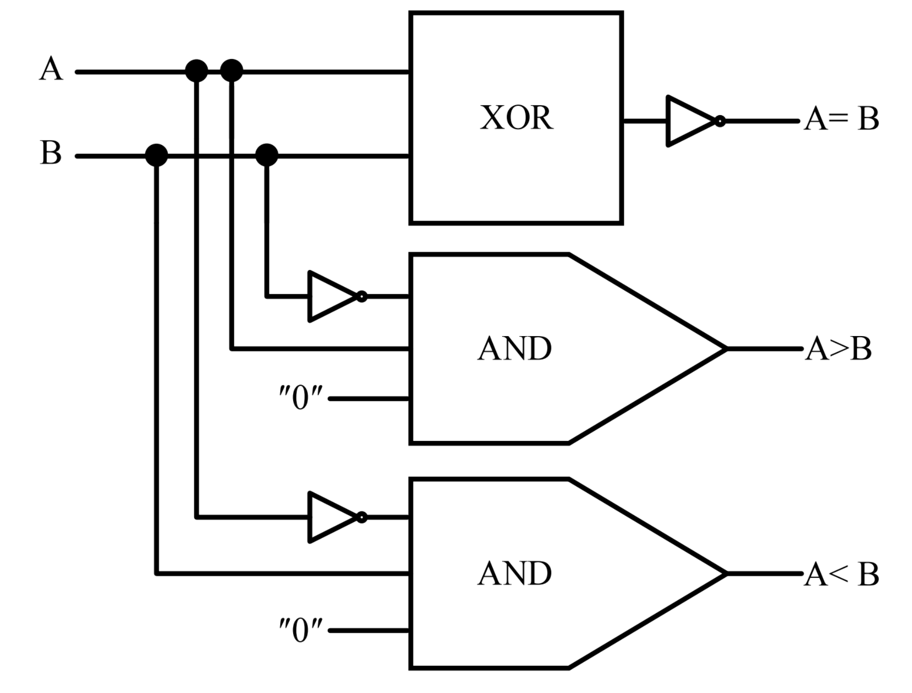
3.4. Design of Reversible 1-Bit Comparator Circuit
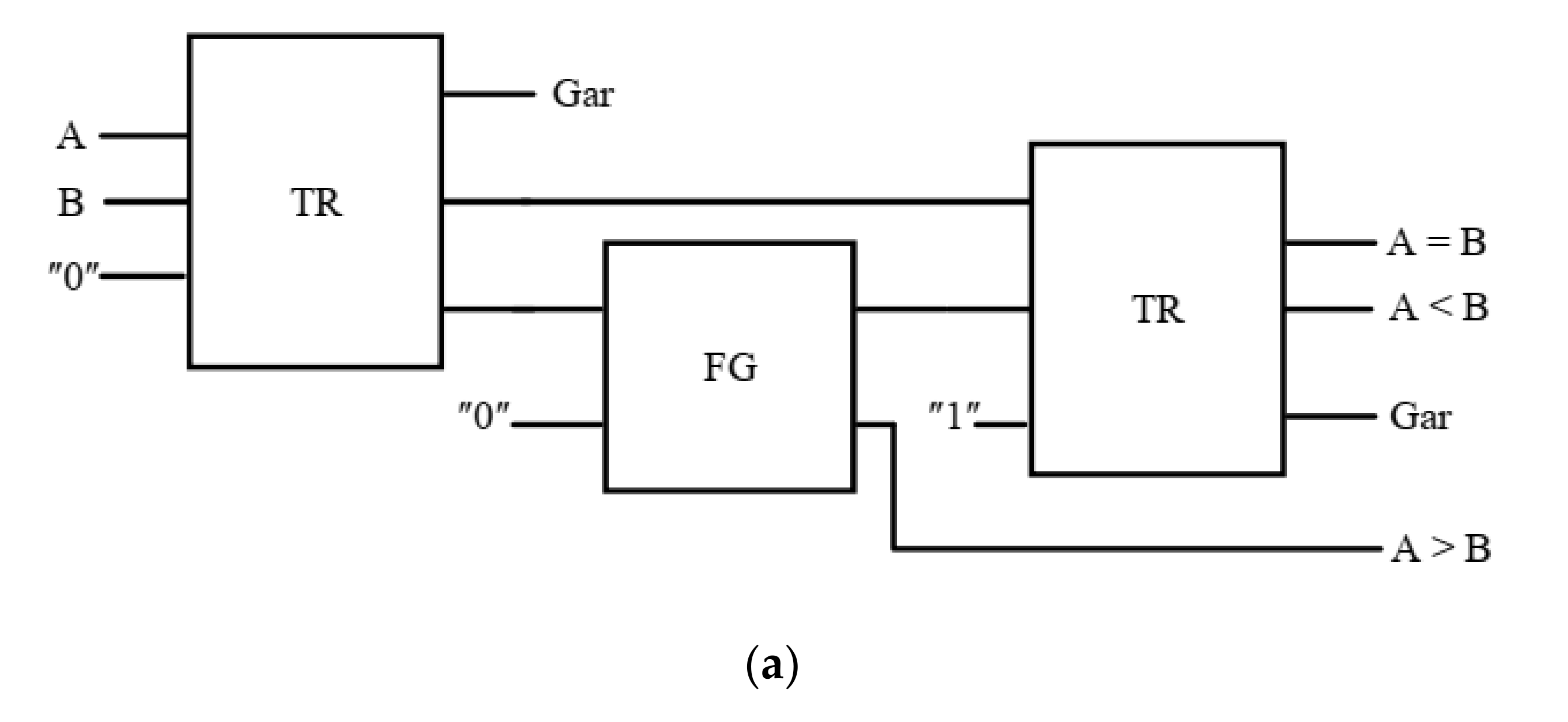
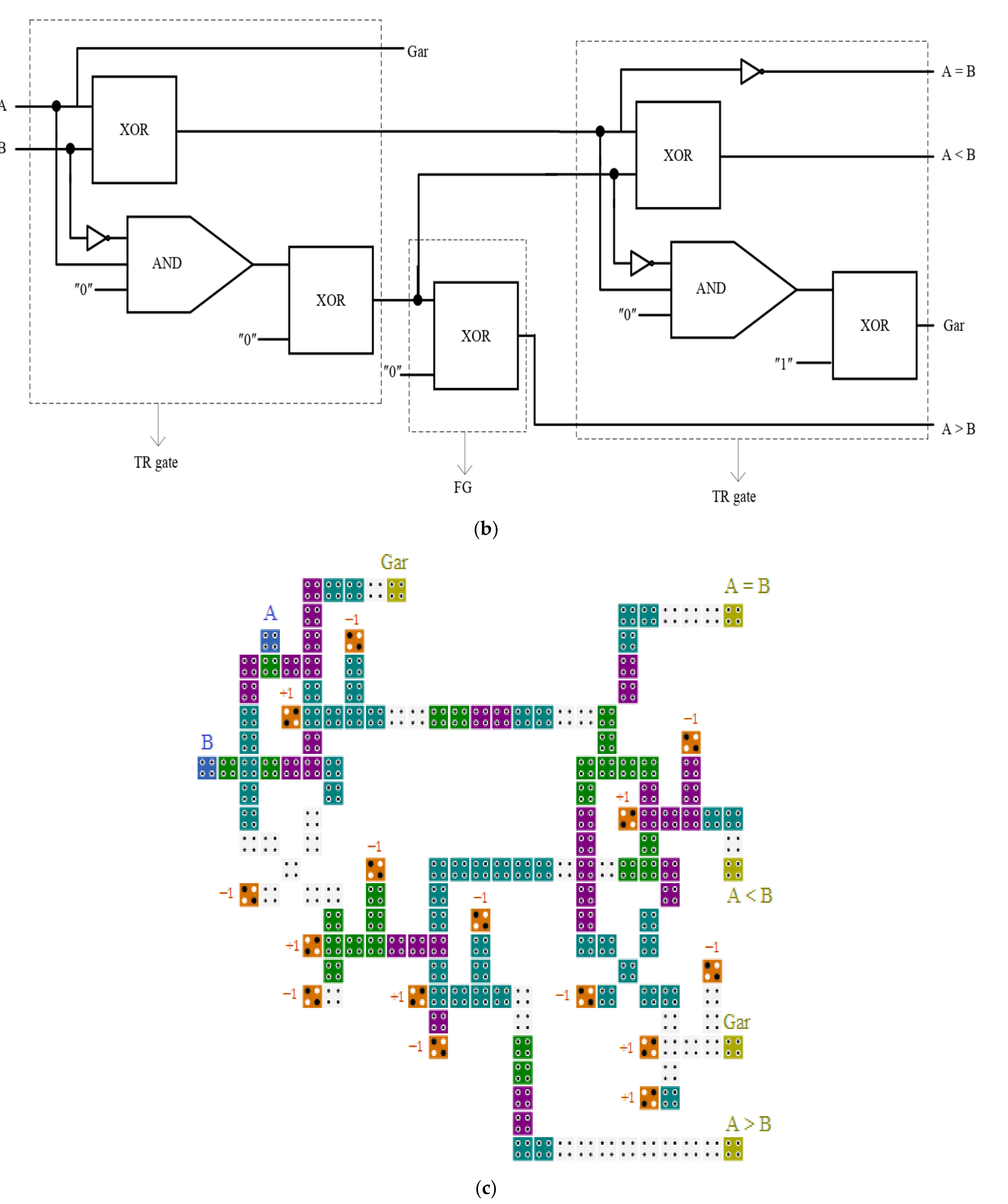
A reversible 1-bit comparator can be built by combining the TR gate and FG, as shown in Figure 11. For its creation and design, it requires two TR gates and one FG gate. As can be seen, the proposed design produces only two waste outlets. The block diagram, logic diagram, and QCA implementation are shown in Figure 11a–c, respectively.
4. Performance Evaluation
4.1. Design Results and Discussions
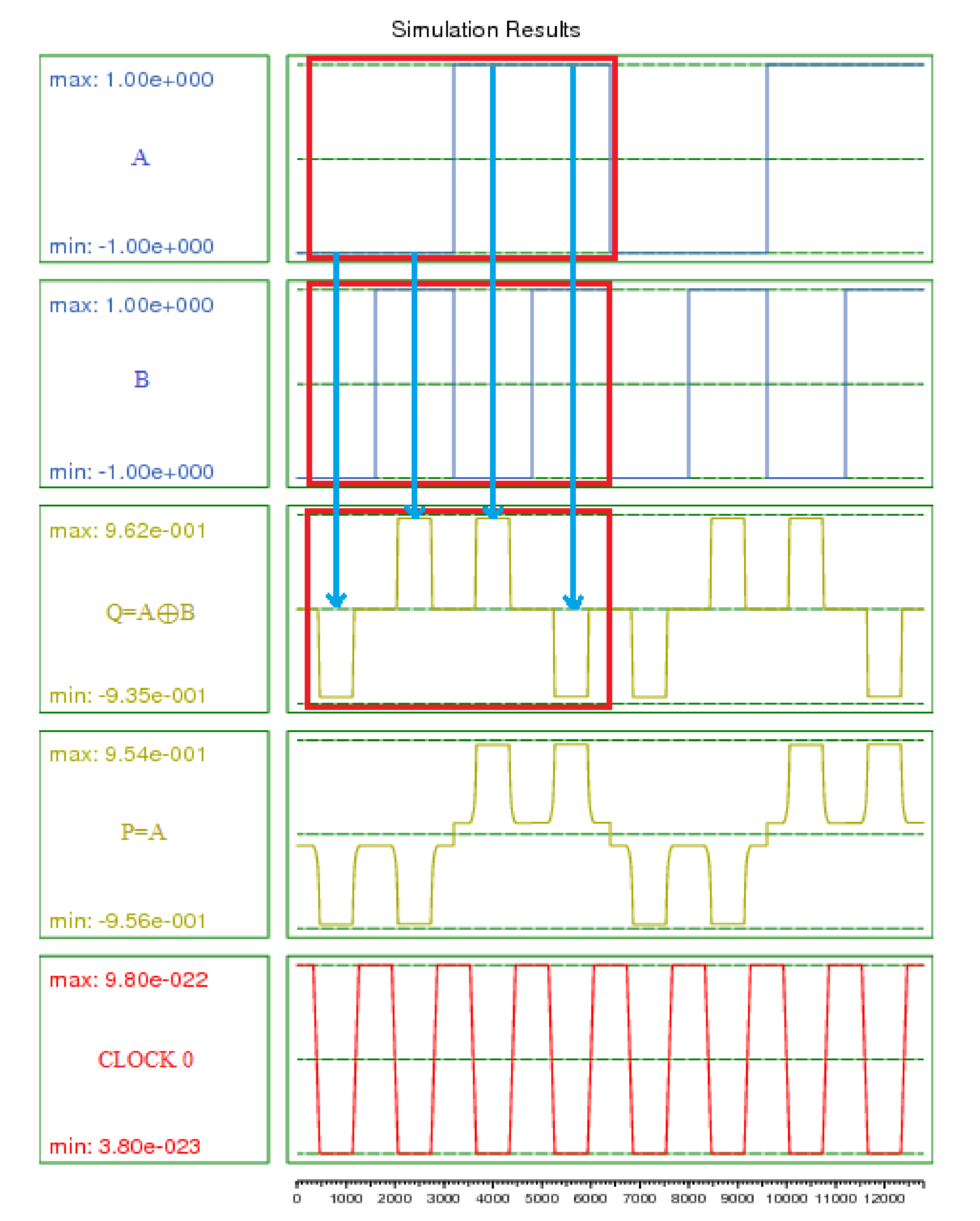
All the designs were simulated and verified using the QCADesiner 2.0.3 version. In our verification process, both the bistable approximation and coherence vector simulation engines have been applied. The list of parameters used is given in Table 4. Figure 12 shows the output of the FG simulation implemented with the simulator. The simulation results are compiled and approved with Table 2. The results show that, against the inputs A = 1 and B = 0, the outputs were P = 1 and Q = 1; against the inputs A = 1 and B = 1, the outputs were P = 1 and Q = 0, as shown in Figure 12. For the remainder of the inputs values, the outputs were correct and similar to the truth table.
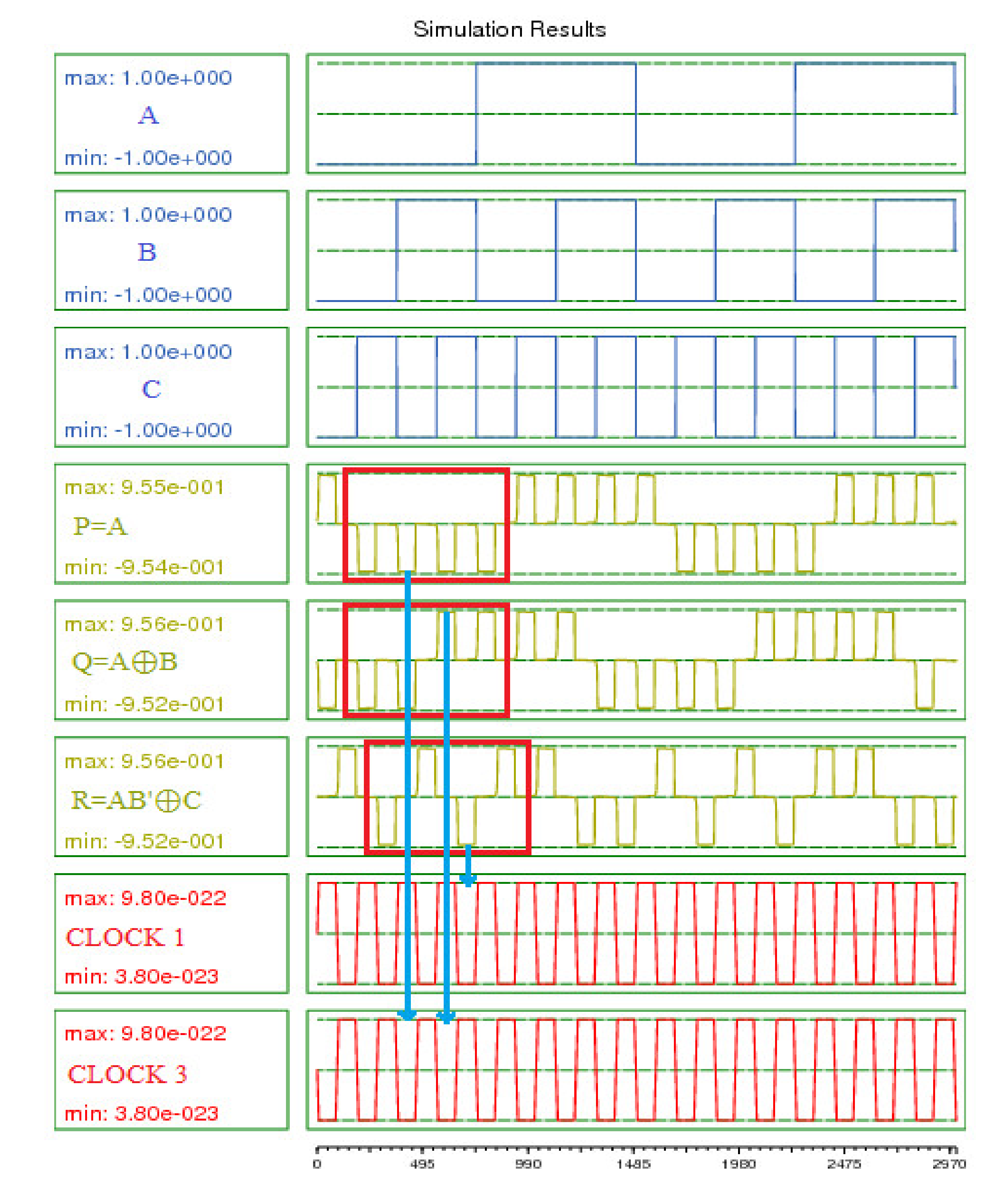
Figure 13 represents the simulation outputs of the TR gate; the results are compiled and approved in Table 3. The results show, against the inputs A = 1, B = 1, and C = 0, the outputs were P = 1, Q = 0, and R = 0; against inputs A = 1, B = 1, and C = 1, the outputs values were P = 1, Q = 0 and R = 1; for the remainder, the outputs were similar to those in Table 3.
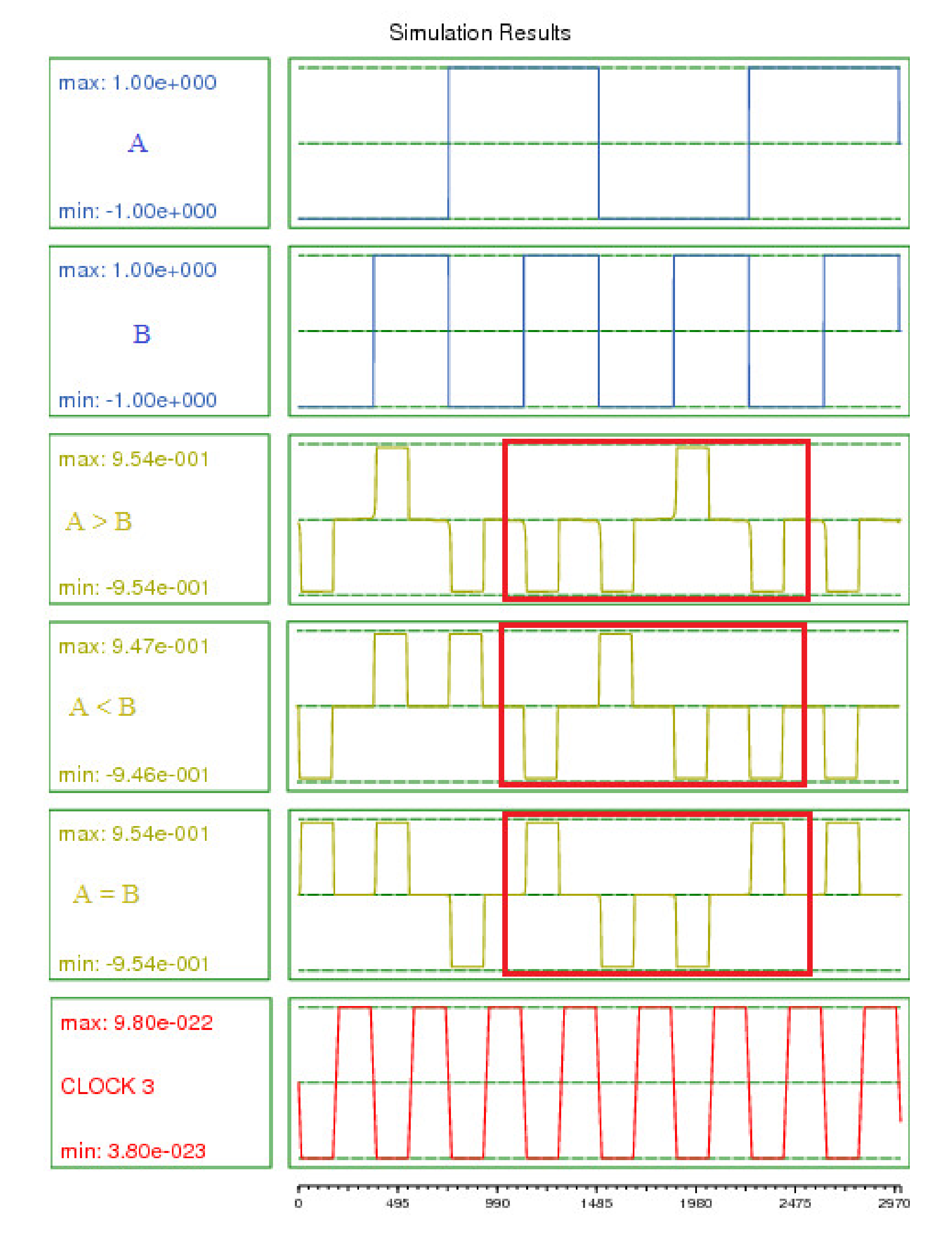
Figure 14 represents the simulation outputs for the proposed one-bit comparator; as be seen, the results are compiled and approved in Table 1. The circuit against the inputs A = 1 and B = 0 had outputs of A > B, A < B, and A = B, respectively, 0, 0, and 1. Against inputs A = 1 and B = 0, outputs were 1, 0 and 0, respectively. For the remainder of the inputs, outputs were similar to those seen in Table 1.
4.2. Results Circuit Cost and Quantum Cost
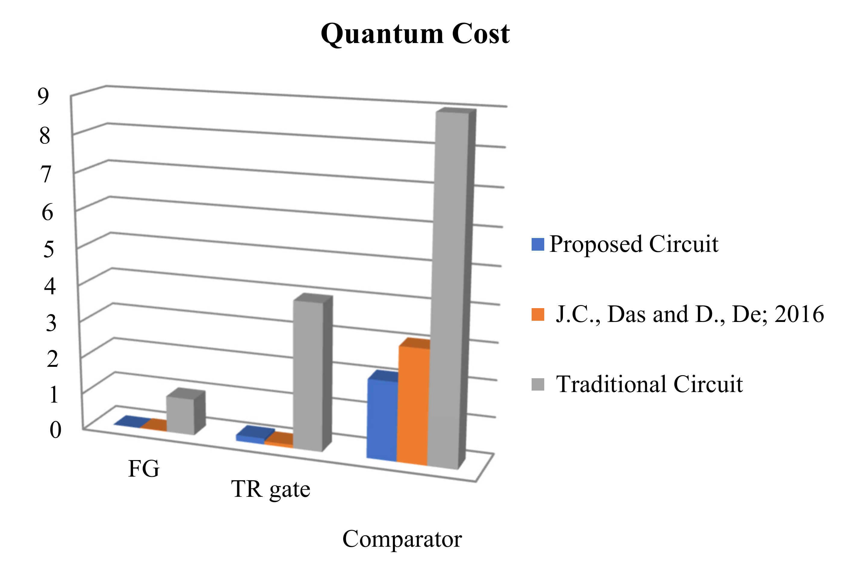
The number of AND, XOR, and NOT operation gates, which were used to create and build each reversible gate or circuit, was referred as the circuit cost. Circuit cost for the FG and TR gates were and , respectively [22]. Where , , and show the number of XOR, AND, and NOT gates, respectively. As shown in Figure 11, the proposed 1-bit reversible comparator circuit was designed with two TR gates, one FG gate, and one NOT gate. Thus, the proposed reversible comparator with two TR gates, one FG gate, and one NOT gate had a circuit cost of and quantum cost of . Thus, 4 was the quantum cost for the TR gate and 1 was the quantum cost for the FG gate. Because two TR gates were used, the cost of the proposed one-bit comparator circuit for the two TR gates and one FG gate was 9. Figure 15 shows the quantum cost required for the performance of the proposed comparator with traditional technology and QCA-based technology, in exchange for our implementation design and [2]. Figure 15 confirms that QCA-based design was less costly than current technology design. Table 5 shows the quantum cost for the proposed reversible circuit. The following equation was used to calculate the quantum cost in QCA technology, where the area is the consumption and occupation area of the QCA circuit and latency is the delay of the QCA circuit.
Table 5 and Table 6 show the quantum cost for QCA implementation and layout of the proposed FG gate, TR gate, and one-bit comparator circuit, as well as a comparison for the proposed QCA reversible circuits by previous work layout. As represented in Table 5 and Table 6, the quantum cost for the comparator circuit was 3.087 for [2], 9 for traditional implementation, and 2.133 for our QCA implementation. As a result, our proposed circuit was 76.3% and 30.9% superior, in terms of the quantum cost of its implementation than with traditional technology and [2], respectively as.
4.3. Complexity Estimation for the Proposed Circuits
Table 7 shows a comparison with the reference design [2]. The QCA implementation for the proposed FG gate for the QCA parameters, such as area, delay, and number of consumed cells had 0.010 µm2 consumption area, 0.25 delay clock, and 11 QCA cells, respectively. For the proposed TR gate, it had 0.073 µm2 consumption area, 1.5 delay clock, and 64 QCA cells, respectively. The QCA circuit for the proposed 1-bit reversible comparator also had 0.237 µm2 consumption area, 3.0 delay clock, and 165 QCA cells, respectively.
On the other hand, considering the design of complex gates and circuits, determining the best way to design the wires crossovers, in order to reduce the cost, is very important [6]. In the design of wires crossovers, the design of coplanar crossovers using non-adjacent clock phases, in addition to being implemented and designed in a single layer, has a lower implementation cost and is the best type, compared to other types of wires crossover implementations. As a result, as compared in the table, all our designs are implemented on a single layer and as a coplanar design. Additionally, the power delay product evaluation criterion (PDP), based on [16], using the QCADesignerE software, is illustrated in Table 7. A frequency of 1 THz was considered to calculate PDP. As can be seen in Table 7, the powers of the proposed FG gate, TR gate, and 1-bit comparator circuit were 11.47 × 10⁻¹⁰, 27.56 × 10⁻¹⁰, and 58.32 × 10− 10 (W), respectively. The proposed FG gate, TR gate, and 1-bit comparator showed improvements of 50.62%, 62.69%, and 63.95%, respectively, in comparison to the power parameter compared to the design [2]. Additionally, the PDP parameters for the proposed FG gate, TR gate, and 1-bit comparator circuit were 2.867 × 10⁻²², 41.34 × 10⁻²², and 174.96 × 10⁻²² (Ws), respectively. As a result, in terms of the PDP parameter, the proposed FG gate, TR gate, and 1-bit comparator circuit, compared to [2], were superior at about 83.54%, 44.03%, and 63.95%, respectively.
4.4. Energy Dissipation Analysis for the Proposed QCA Layout Circuits
In the calculations, the same power dissipation is considered for all cells. So, in a clock cycle, the average total power dissipation for the QCA circuits is estimated by considering the total power dissipation of all NOT and MV gates [23].
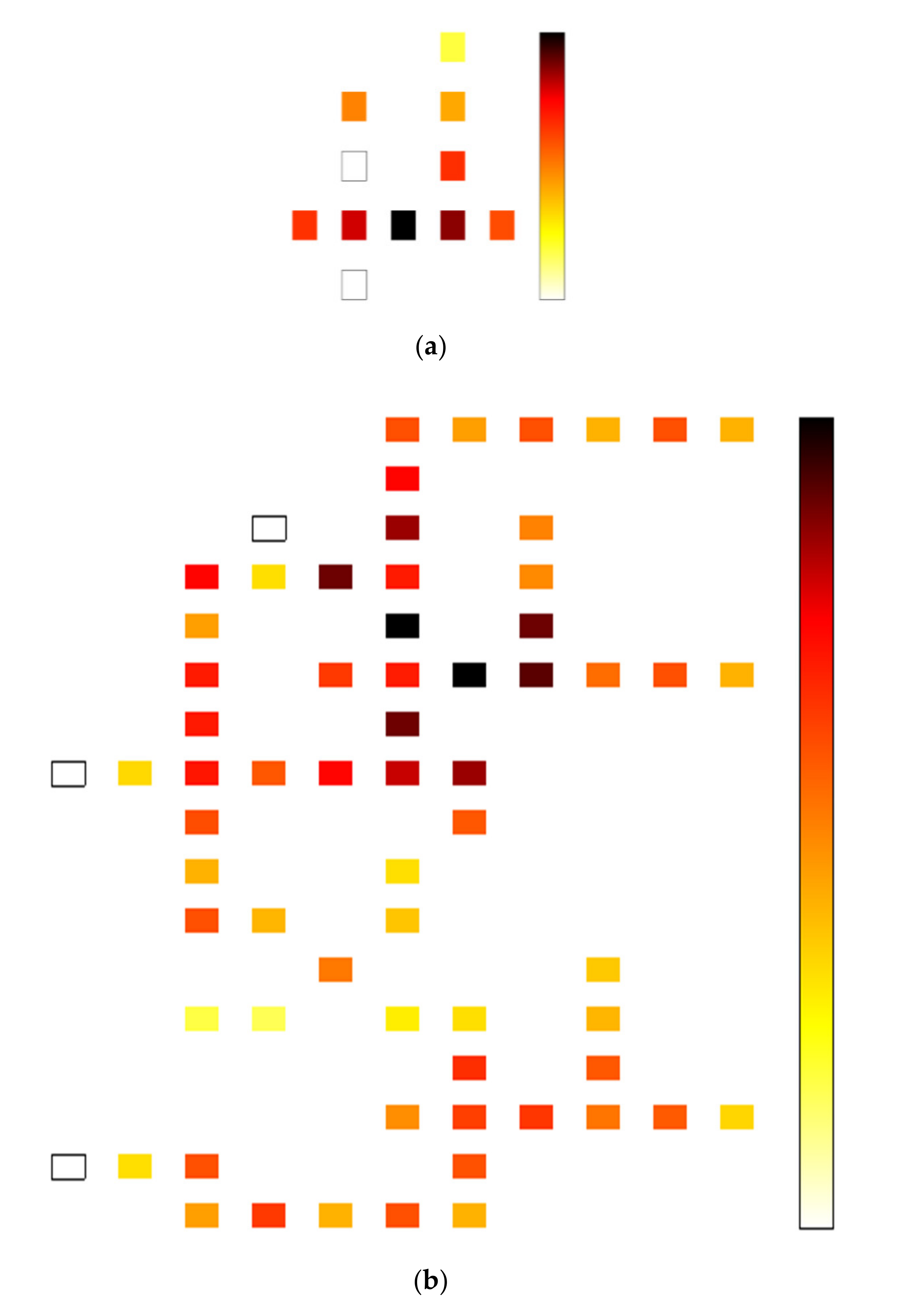
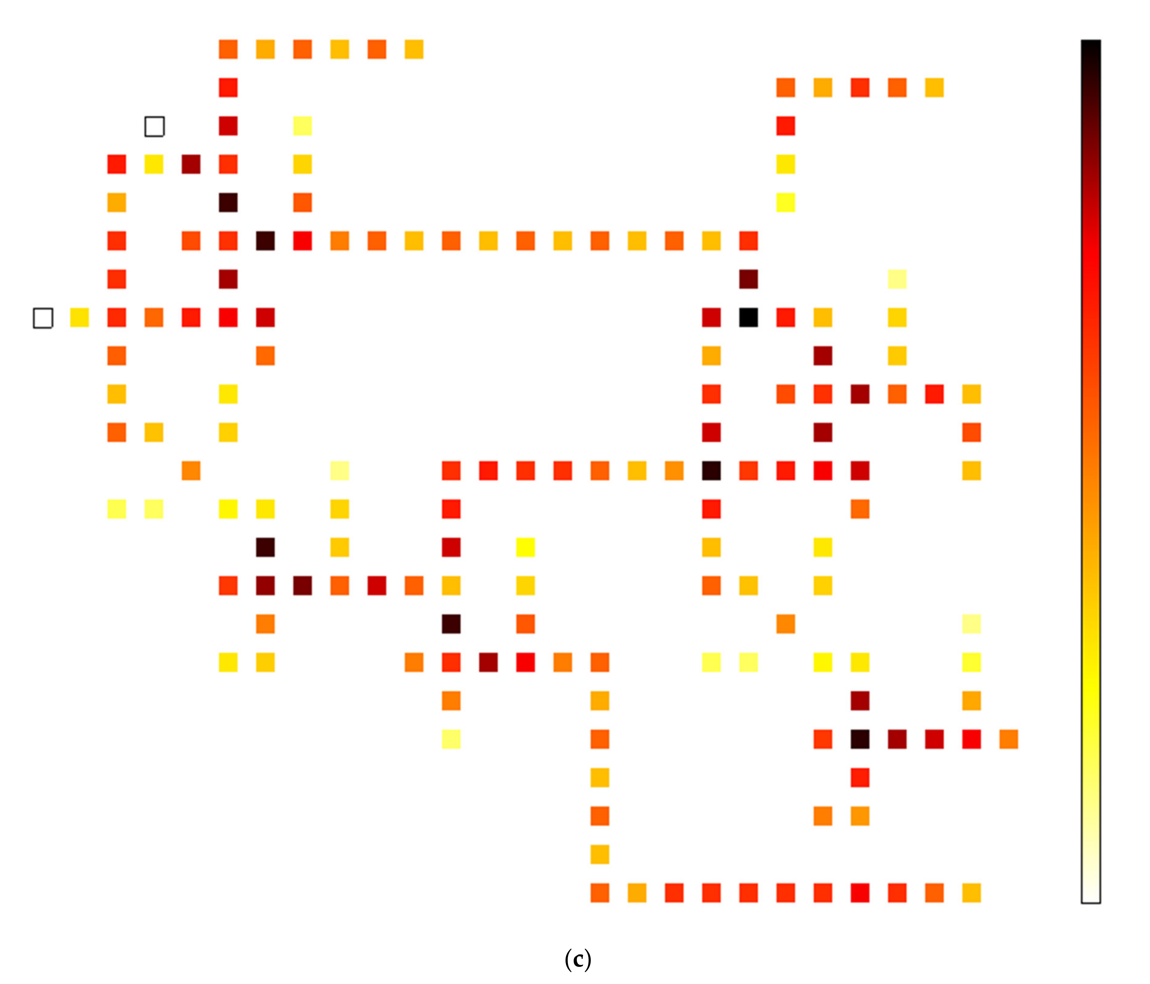
In the method reported in [23], T = 2.0 K for different tunneling energies has been used to estimate the power dissipation of QCA circuits. The results of the power dissipation measurements are shown in Table 8. As can be seen, power dissipation provided for tunneling energy (0.5, 1.0, and 1.5 Ek). Figure 16 also shows the power dissipation measurement of the proposed circuits implemented with QCA using QCAPro [24], as well as the power loss of the (A) Fayman gate, (B) TR gate, and (C) one-bit comparator circuit using QCAPro tool.
5. Conclusions
This paper describes the advanced and optimal design of the FG and TR gates using QCA. Using these two optimal designs, we design a reversible and cost-effective 1-bit quantum comparator. The proposed 1-bit reversible comparator implemented with QCA was denser and had less cell consumption and latency than the previous works. Comparison analysis for the proposed novel 1-bit reversible comparator with others showed a cost-effective novel circuit, in terms of quantum cost and the main QCA parameters. The reversible QCA comparator has a very low power dissipation than the compared sample. The simulation results for the novel reversible comparator circuit implemented with QCA were confirmed by the truth table, which validated the operational efficiency of the proposed novel design. The comparator circuits in the performance of other computational operations and their usage in the design of microcontrollers and CPUs are very important. The novel circuit can be used to create more complex circuits, reduce quantum cost, reduce circuit cost, and encourage optimization.
Author Contributions
Conceptualization, M.V.; methodology, M.V.; software, M.V. and A.N.B.; validation, M.V., A.N.B., P.L., and A.O.; formal analysis, M.V.; investigation, M.V., A.N.B., P.L., and A.O.; resources, M.V. and A.N.B.; data curation, M.V.; writing—original draft preparation, M.V.; writing—review and editing, A.N.B., P.L., A.O., and K.A.W.; supervision, A.N.B., P.L., A.O., and K.A.W. All authors have read and agreed to the published version of the manuscript.
Funding
This research received no external funding.
Institutional Review Board Statement
Not applicable.
Informed Consent Statement
Not applicable.
Data Availability Statement
Not applicable.
Conflicts of Interest
The authors declare no conflict of interest.
References
- D’Ariano, G.M.; Perinotti, P. Quantum cellular automata and free quantum field theory. Front. Phys. 2017, 12, 1–11. [Google Scholar] [CrossRef] [Green Version]
- Das, J.C.; De, D. Reversible comparator design using quantum dot-cellular automata. IETE J. Res. 2016, 62, 323–330. [Google Scholar] [CrossRef]
- Thapliyal, H.; Ranganathan, N. Reversible logic-based concurrently testable latches for molecular QCA. IEEE Trans. Nanotechnol. 2010, 9, 629. [Google Scholar] [CrossRef]
- Nower, N.; Chowdhury, A.R. Design and analysis of a compact reversible ternary systolic array. Int. J. Comput. Electr. Eng. 2011, 3, 8905. [Google Scholar] [CrossRef]
- Arjmand, M.M.; Soryani, M.; Navi, K. Coplanar wire crossing in quantum cellular automata using a ternary cell. IET Circuits Devices Syst. 2013, 7, 26372. [Google Scholar] [CrossRef]
- Das, J.C.; Debnath, B.; De, D. Image steganography using quantum-dot cellular automata. Quantum Matter 2015, 4, 50417. [Google Scholar] [CrossRef]
- Vahabi, M.; Lyakhov, P.; Bahar, A.N. Design and Implementation of Novel Efficient Full Adder/Subtractor Circuits Based on Quantum-Dot Cellular Automata Technology. Appl. Sci. 2021, 11, 8717. [Google Scholar] [CrossRef]
- Lent, C.S.; Tougaw, P.D. A device architecture for computing with quantum dots. Proc. IEEE 1997, 85, 541–557. [Google Scholar] [CrossRef] [Green Version]
- Lent, C.S.; Tougaw, P.D. Lines of interacting quantum-dot cells: A binary wire. J. Appl. Phys. 1993, 74, 6227–6233. [Google Scholar] [CrossRef] [Green Version]
- Vahabi, M.; Bahar, A.N.; Otsuki, A.; Wahid, K.A. Ultra-Low-Cost Design of Ripple Carry Adder to Design Nanoelectronics in QCA Nanotechnology. Electronics 2022, 11, 2320. [Google Scholar] [CrossRef]
- Landauer, R. Irreversibility and heat generation in the computing process. IBM J. Res. Dev. 1961, 5, 183–191. [Google Scholar] [CrossRef]
- Bennett, C.H. Logical reversibility of computation. IBM J. Res. Dev. 1973, 17, 525–532. [Google Scholar] [CrossRef]
- Gin, A.; Tougaw, P.D.; Williams, S. An alternative geometry for quantum-dot cellular automata. J. Appl. Phys. 1999, 85, 8281–8286. [Google Scholar] [CrossRef]
- Walus, K.; Jullien, G.A. Design tools for an emerging soc technology: Quantum-dot cellular automata. Proc. IEEE 2006, 94, 1225–1244. [Google Scholar] [CrossRef]
- Shin, S.-H.; Jeon, J.-C.; Yoo, K.-Y. Wire-crossing technique on quantum-dot cellular automata, in NGCIT2013, the 2nd International Conference on Next Generation Computer and Information Technology. Comput. Sci. 2013, 27, 52–57. [Google Scholar]
- Vahabi, M.; Lyakhov, P.; Bahar, A.N.; Wahid, K.A. Design and Implementation of New Coplanar FA Circuits without NOT Gate and Based on Quantum-Dot Cellular Automata Technology. Appl. Sci. 2021, 11, 12157. [Google Scholar] [CrossRef]
- Das, J.C.; De, D. Reversible half-adder design using QCA. In Quantum Matter; American Scientific Publishers: Valencia, CA, USA, 2016. [Google Scholar]
- Das, K.; De, D. Characterization, test and logic synthesis of novel conservative & reversible logic gates for QCA. Int. J. Nanosci. 2010, 9, 20114. [Google Scholar]
- Thapliyal, H.; Ranganathan, N.; Kotiyal, S. Design of testable reversible sequential circuits. IEEE Trans. 2013, 21, 12019. [Google Scholar] [CrossRef]
- Dehghan, B.; Roozbeh, A.; Zare, J. Design of low power comparator using DG gate. Circuits Syst. Sci. Res. 2014, 5, 712. [Google Scholar] [CrossRef] [Green Version]
- Thapliyal, H.; Ranganathan, N. Design of efficient reversible binary subtractors based on a new reversible gate. In Proceedings of the IEEE Computer Society Annual Symposium on VLSI, Washington, DC, USA, 13–15 May 2009; p. 22934. [Google Scholar]
- Moallem, P.; Ehsanpour, M. A novel design of reversible multiplier circuit. Int. J. Eng. 2013, 26, 57786. [Google Scholar] [CrossRef]
- Liu, W.; Srivastava, S.; Lu, L.; O’Neill, M.; Swartzlander, E.E. Are QCA cryptographic circuits resistant to power analysis attack? IEEE Trans. Nanotechnol. 2012, 11, 123951. [Google Scholar] [CrossRef]
- Srivastava, S.; Asthana, A.; Bhanja, S.; Sarkar, S. QCAPro-an error-power estimation tool for QCA circuit design. In Proceedings of the 2011 IEEE International Symposium of Circuits and Systems (ISCAS), Rio de Janeiro, Brazil, 15–18 May 2011. [Google Scholar]
Figure 1.
Schematics types of QCA cells (a) two structures logical values the QCA 90-degree cells, (b) QCA 90-degree wire, (c) two structures logical values the QCA 45-degree cells, (d) QCA 45-degree wire.
Figure 1.
Schematics types of QCA cells (a) two structures logical values the QCA 90-degree cells, (b) QCA 90-degree wire, (c) two structures logical values the QCA 45-degree cells, (d) QCA 45-degree wire.

Figure 2.
The four-phase clock.

Figure 3.
QCA crossover, (a) multilayer crossovers, (b) coplanar crossovers by using rotation cells, and (c) coplanar crossover by using standard cells.
Figure 3.
QCA crossover, (a) multilayer crossovers, (b) coplanar crossovers by using rotation cells, and (c) coplanar crossover by using standard cells.


Figure 4.
(a) MV, (b) two-input AND, (c) two-input OR, and (d) inverter gates.

Figure 5.
Block diagram logic circuit 1-bit comparator.

Figure 6.
The quantum implementation (a) inverter, (b) control V, and (c) control V+.

Figure 7.
The quantum implementation FG.

Figure 8.
FG gate (a) logic diagram, (b) block diagram, and (c) QCA layout.

Figure 9.
The quantum implementation TR gate.

Figure 10.
TR gate (a) logic diagram, (b) block diagram, and (c) QCA layout.


Figure 11.
The 1-bit comparator (a) logic diagram, (b) block diagram, and (c) QCA layout.


Figure 12.
Simulation results for FG gate.

Figure 13.
Simulation results for TR gate.

Figure 14.
Simulation results for the proposed 1-bit comparator.

Figure 15.
Quantum cost for the proposed circuits [2].
Figure 15.
Quantum cost for the proposed circuits [2].

Figure 16.
Thermal hotspots of the (a) FG gate, (b) TR gate, and (c) reversible 1-bit comparator at 0.5 Ek.
Figure 16.
Thermal hotspots of the (a) FG gate, (b) TR gate, and (c) reversible 1-bit comparator at 0.5 Ek.


Table 1.
Truth table of one-bit comparator.
| Input | Output | |||
|---|---|---|---|---|
| A | B | A > B | A < B | A = B |
| 0 | 0 | 0 | 0 | 1 |
| 0 | 1 | 0 | 1 | 0 |
| 1 | 0 | 1 | 0 | 0 |
| 1 | 1 | 0 | 0 | 1 |
Table 2.
Truth table of FG.
| Input | Output | ||
|---|---|---|---|
| A | B | P | Q |
| 0 | 0 | 0 | 0 |
| 0 | 1 | 0 | 1 |
| 1 | 0 | 1 | 1 |
| 1 | 1 | 1 | 0 |
Table 3.
Truth table of TR gate.
| Input | Output | ||||
|---|---|---|---|---|---|
| A | B | C | P | Q | R |
| 0 | 0 | 0 | 0 | 0 | 0 |
| 0 | 0 | 1 | 0 | 0 | 1 |
| 0 | 1 | 0 | 0 | 1 | 0 |
| 0 | 1 | 1 | 0 | 1 | 1 |
| 1 | 0 | 0 | 1 | 1 | 1 |
| 1 | 0 | 1 | 1 | 1 | 0 |
| 1 | 1 | 0 | 1 | 0 | 0 |
| 1 | 1 | 1 | 1 | 0 | 1 |
Table 4.
Simulation parameters of the coherence vector tool.
| Parameter | Value |
|---|---|
| Cell width | 18 nm |
| Cell height | 18 nm |
| Relative permittivity | 12.9 |
| Dot diameter | 5 nm |
| Number of samples | 12,800 |
| Convergence tolerance | 0.001 |
| Clock high | 9.8 × 10⁻²² J |
| Clock low | 3.8 × 10⁻²³ J |
| Clock amplitude factor | 2 |
| Radius of effect | 65 nm |
| Layer separation | 11.5 nm |
| Maximum iteration per sample | 100 |
Table 5.
Quantum cost for the proposed reversible circuits.
| Proposed Reversible Circuits | Area (µm2) | Latency (clock) | Cost (Area × Latency2) |
|---|---|---|---|
| FG | 0.010 | 0.25 | 0.0006 |
| TR gate | 0.073 | 1.50 | 0.164 |
| 1-bit comparator | 0.237 | 3.0 | 2.133 |
Table 6.
Quantum cost for QCA layout the proposed reversible circuits.
| Proposed Reversible Circuits | Circuit Cost | Quantum Cost |
|---|---|---|
| FG | 1 | |
| TR gate | 4 | |
| 1-bit comparator | 9 |
Table 7.
Comparison for the proposed QCA reversible circuits of previous works.
| Proposed Reversible Circuits | Area (µm2) | Cell Count | Delay (Clock) | Cost (Area × Latency2) | Power (W) | PDP (Ws) (Power × Latency) | Crossover Type |
|---|---|---|---|---|---|---|---|
| FG [2] | 0.023 | 37 | 0.75 | 0.013 | 23.23 × 10⁻¹⁰ | 17.42 × 10⁻²² | Multi-Layer |
| TR gate [2] | 0.090 | 122 | 1.0 | 0.090 | 73.86 × 10⁻¹⁰ | 73.86 × 10⁻²² | Multi-Layer |
| 1-bit comparator [2] | 0.343 | 319 | 3.0 | 3.087 | 161.8 × 10⁻¹⁰ | 485.4 × 10⁻²² | Multi-Layer |
| Proposed FG | 0.010 | 11 | 0.25 | 0.0006 | 11.47 × 10⁻¹⁰ | 2.867 × 10⁻²² | Coplanar |
| Proposed TR gate | 0.073 | 64 | 1.5 | 0.164 | 27.56 × 10⁻¹⁰ | 41.34 × 10⁻²² | Coplanar |
| Proposed 1-bit comparator | 0.237 | 165 | 3.0 | 2.133 | 58.32 × 10⁻¹⁰ | 174.96 × 10⁻²² | Coplanar |
Table 8.
Comparison for the proposed QCA reversible circuits by previous works.
| Proposed Reversible Circuits | Avg Leakage Energy (meV) | Avg Switching Energy (meV) | Avg Energy Diss (meV) | ||||||
|---|---|---|---|---|---|---|---|---|---|
| 0.5 EK | 1 EK | 1.5 EK | 0.5 EK | 1 EK | 1.5 EK | 0.5 EK | 1 EK | 1.5 EK | |
| FG | 3.78 | 10.42 | 17.82 | 10.54 | 9.22 | 7.98 | 14.32 | 19.64 | 25.80 |
| TR gate | 21.42 | 63.10 | 110.65 | 89.03 | 76.12 | 64.38 | 110.45 | 139.22 | 175.03 |
| 1-bit comparator | 53.82 | 162.65 | 287.96 | 267.05 | 230.20 | 195.15 | 320.87 | 392.85 | 483.11 |
Publisher’s Note: MDPI stays neutral with regard to jurisdictional claims in published maps and institutional affiliations. |
© 2022 by the authors. Licensee MDPI, Basel, Switzerland. This article is an open access article distributed under the terms and conditions of the Creative Commons Attribution (CC BY) license (https://creativecommons.org/licenses/by/4.0/).
Share and Cite
MDPI and ACS Style
Vahabi, M.; Lyakhov, P.; Bahar, A.N.; Otsuki, A.; Wahid, K.A. Novel Reversible Comparator Design in Quantum Dot-Cellular Automata with Power Dissipation Analysis. Appl. Sci. 2022, 12, 7846. https://doi.org/10.3390/app12157846
AMA Style
Vahabi M, Lyakhov P, Bahar AN, Otsuki A, Wahid KA. Novel Reversible Comparator Design in Quantum Dot-Cellular Automata with Power Dissipation Analysis. Applied Sciences. 2022; 12(15):7846. https://doi.org/10.3390/app12157846
Chicago/Turabian StyleVahabi, Mohsen, Pavel Lyakhov, Ali Newaz Bahar, Akira Otsuki, and Khan A. Wahid. 2022. "Novel Reversible Comparator Design in Quantum Dot-Cellular Automata with Power Dissipation Analysis" Applied Sciences 12, no. 15: 7846. https://doi.org/10.3390/app12157846
Note that from the first issue of 2016, this journal uses article numbers instead of page numbers. See further details here.