
Abstract
From ripples to defects, edges and grain boundaries, the 3D atomic structure of 2D materials is critical to their properties. However the damage inflicted by conventional 3D analysis precludes its use with fragile 2D materials, particularly for the analysis of local defects. Here we dramatically increase the potential for precise local 3D atomic structure analysis of 2D materials, with both greatly improved dose efficiency and sensitivity to light elements. We demonstrate light atoms can now be located in complex 2D materials with picometer precision at doses 30 times lower than previously possible. Moreover we demonstrate this using WS2, in which the light atoms are practically invisible to conventional methods at low doses. The key advance is combining the concept of few tilt tomography with highly dose efficient ptychography in scanning transmission electron microscopy. We further demonstrate the method experimentally with the even more challenging and newly discovered 2D CuI, leveraging a new extremely high temporal resolution camera.
Export citation and abstract BibTeX RIS

Original content from this work may be used under the terms of the Creative Commons Attribution 4.0 license. Any further distribution of this work must maintain attribution to the author(s) and the title of the work, journal citation and DOI.
1. Introduction
Since the first isolation of graphene [1], the outstanding properties of 2D materials have attracted huge attention. These properties emerge from their single atom or single unit cell thicknesses and make them promising candidates for a wide variety of applications including electronics, optoelectronics, energy storage devices, and ultra-sensitive detectors [2, 3]. However, despite their name, the properties of 2D materials are in fact determined by their 3D structures. For example, perfectly flat graphene is unstable [4]. The famous stability of the material originates from its 3D structure [5]. Such examples of the importance of the 3D structure of 2D materials are ubiquitous [6–10]. Not only do these materials easily deform out of plane to accommodate strain or defects, but they also frequently consist of three or more atomic layers, with this number increased multiple times in vertical heterostructures. Thus it should be no surprise that the 3D structure of 2D materials can dramatically alter their properties.
3D structures are typically determined with tomography. For atomic resolution this requires either atom probe tomography (APT) or electron tomography in a scanning transmission electron microscope (STEM), but neither are well suited to 2D materials. APT requires samples be formed into sharp needles rather than 2D sheets [11], and conventional electron tomography [12, 13] generally requires prohibitively large electron doses. The lengthy tilt series used by conventional tomography require a hundred times or more dose than a single image [14–16]. Extensions to conventional tomography methods such as GENFIRE [17] have enabled an impressive reduction in the number of tilt angles required from several dozens of tilt angles to as little as 13 tilt angles being sufficient for picometer precision 3D structure determination of pristine single layer MoS2 [18]. However, as impressive as this is, significant barriers remain for 3D structure determination of 2D materials generally. The total dose needs to be further reduced for many materials, especially when looking at features that tend to be of greatest interest, such as defects, edges and interfaces, which are generally far less stable than the bulk structures. Even the simple assignment of atoms within a unit cell can be a difficult task with a limited dose budget. Greater sensitivity to light elements is also needed, a problem that is far worse when the light elements are neighbouring heavy elements. While MoS2 is somewhat beam sensitive, all the atoms can be relatively easily resolved by annular dark field (ADF) atomic number contrast imaging because they do not differ too greatly in atomic number. Even in many pristine 2D materials this is not the case. These aspects are compounded when the materials systems become more complex such as in 2D materials systems with more atomic layers in their unit cells, and 2D heterostructures.
To overcome these barriers we introduce the concept of few tilt ptychotomography. Here we define few tilt tomography as the method of tracking the motion of each individual atom in a material with respect to tilt angle which enables 3D structures to be determined with as few as two tilt angles [19]. Previously the method has been used to determine the 3D structure of relatively robust defects in graphene using the ADF imaging modality alone. Here we greatly increase the capabilities of the few tilt method with the addition of simultaneous ptychography. Ptychography provides far greater overall dose efficiency and ability to simultaneously detect heavy and light elements. Nevertheless, the sensitivity of the ADF signal to atomic number remains extremely useful, and complements the ptychography in our few tilt ptychotomography. Using simulations we demonstrate few tilt ptychotomography is able to determine the 3D structure of WS2 at picometer precision at a dose 30 times lower than that demonstrated for MoS2, despite the S atoms in the WS2 being all but invisible to the ADF signal at such doses in the WS2. Conventional tomographic methods which rely solely on the ADF signal therefore would not be able to provide the same level of precision as seen in MoS2 at even the same dose performed in [18] yet alone at the 30 times lower dose shown here. We provide experimental proof of the capabilities of the method using the new 2D material, CuI, which is more complex than TMDs, making use of an extremely high temporal resolution camera [20] that enables us to perform very rapid low dose 4D STEM indeed. Rapid scans are important to avoid scan distortions, sample drift and other instabilities which could cause artifacts in the 3D reconstruction [19]. This experimental ability provides the key to unlocking the connection between structure and function in new and emerging 2D materials, most of which are predicted to possess complex 3D structures [21]. CuI is more complex than TMDs because the unit cell contains four atomic layers instead the three layers found in TMDs such as WS2. The extra atomic layer results in more overlapping atoms in the tilted projection.
2. Few-tilt ptychotomography of WS2
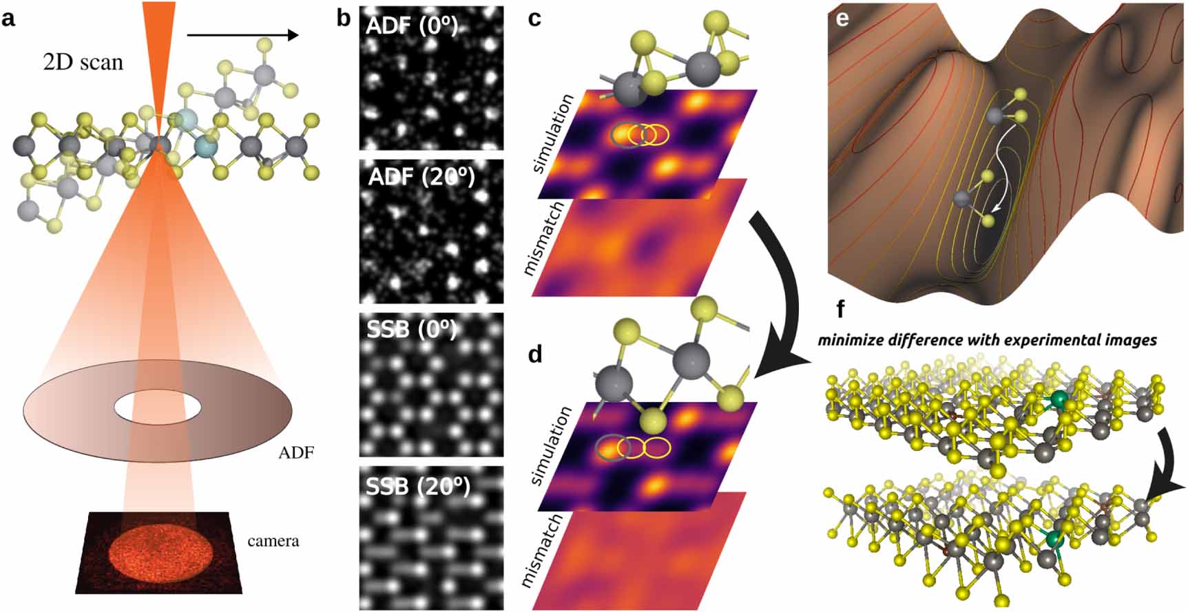
The experimental setup is illustrated in figure 1(a), and consists of obtaining simultaneous 4D STEM and ADF data at each tilt angle. We introduce the method with defective monolayer WS2 data simulated at an electron dose of 
 Å−2 per tilt angle. The first task is to initialize a 2D model with the correct elements and their lateral positions. This is performed by analysing the phases and intensities of the zero tilt SSB and ADF images [22, 23]. At this electron dose the heavy W atoms are clearly visible in the ADF images but the lighter S atoms are not (figure 1(b)). All the elements are however clearly visible in the ptychographic single side band (SSB) images. The vacancies and substitutional C and Nb atoms can also be distinguished (see supplementary figure 2).

Figure 1. Few tilt ptychotomography. (a), Schematic (b), Simulated ADF and SSB images of WS2 at a sample tilt of 0 and 20 degrees, respectively. (c), (d) Simulation of tilted models (wrong and correct S coordinates on (c) and (d), respectively). The circles in the simulation indicate the projected positions and the mismatch is the difference between the simulation and the corresponding target image (experimental image). (e), Correlation landscape of a single atom computed as the negative correlation between simulation and experiment. (f), Initialized (top) and optimized (bottom) model.
Download figure:
Standard image High-resolution imageThe 3D structure is solved by optimising the match between the input images and images simulated based on the initialized model. Both, the model and the imaging conditions used in the simulations based on it are iteratively updated to maximise the correlation. An initial model with the correct lateral positions and elemental identification can typically be obtained from the untilted ADF and ptychographic images. The quantitative Z-contrast of the ADF signal is particularly beneficial to the elemental identification, even with very noisy images. Initial vertical positions can be assigned as flat or use prior knowledge. For the WS2 we assigned an arbitrary offset of z = 1.5 Å between the S atoms with one of the S planes aligned vertically with the W atoms as illustrated in supplementary figure 3. With the initial model established, optimisation is performed using the data from each tilt angle, iteratively updating the position of each atom. In addition to the tilt angle, the source-size broadening, linear drift, scan distortions and atomic scattering factors are included as adjustable parameters to obtain the best match.
As in all tomography, the shift of an atom in the projected image upon tilting is used to infer its 3D position. This shift is apparent in the ptychographic SSB input image shown in figure 1(b) with the sample tilted to 20∘, and in the SSB images simulated from the models shown in figure 1(c). As the WS2 model is optimised, the lower layer of S atoms extends further below the plane of the W atoms, causing the locations of the atoms to spread out laterally from the initial configuration in (c) to the final optimised positions in (d). Maps of the mismatch between the ptychographic images from these configurations and the input image at this tilt are also displayed in parts c and d. With the lower S atom too close to the W plane, the projected W and S positions are also too close together and the mismatch is significant. As the lower S atom extends further below the W plane towards the position typical for TMDs, the projected positions of the atoms spreads out and the mismatch is reduced.
The optimisation is further illustrated in figure 1(e) with a 3D rendering of the negative correlation of the match between the input and simulated data vs the position of the lower S atom in one of the WS2 units. The correlation potential landscape of a single S atom was calculated by shifting it in all directions and tracking the merit function. A sharp valley appears where an optimisation algorithm can easily determine the correct atomic position by simple minimisation. Since the potential landscape depends on the other atoms of the system, the optimisation is iterated atom-by-atom in multiple cycles. When all atomic positions are converged, the final model shows an excellent match with the input model.
Using simulations and a predefined target model allows us to quantify the accuracy and precision of the method by calculating the difference between the target and optimised models. Our calculations show that the method can provide a precision in the low picometer range under low-dose conditions. We obtain a precision of 4.8 pm for the heavy W and Nb atoms at 
 Å−2. As the heavier elements produce a stronger signal than lighter elements in the ADF images, they are able to be located with greater precision. The best precision previously achieved for S atoms in a TMD was 15 pm using a total dose of
 Å−2 [18] and 13 tilt angles. Our few tilt ptychotomography method achieves this specific precision with only 3 tilts and 1/30th the total dose despite WS2 being a far more difficult material in which to locate light atoms than the MoS2 used by Tian et al Compared to the Mo in MoS2, the near factor of two increase in atomic number of the W makes the S2 atoms all but invisible in ADF images of WS2, but the ptychography shows them clearly at this dose. The statistical relationship between the number of tilt angles and the precision is discussed in detail in the supplementary information for the full defected structure which includes very light C atoms.
3. Experimental example: 2D CuI
We now apply the method to an experimental data set from monolayer hexagonal CuI. This new 2D material has very recently been discovered, and is stabilised between two graphene layers [24]. Structurally, it is equivalent to a single layer of β-CuI, with each atomic column containing one Cu and one I atom. Therefore the structure appears as a simple honeycomb lattice when untilted, as shown in the high 
 Å−2 dose ADF image displayed in figure 2(a).

Figure 2. Characterization of 2D CuI. (a), High, 
 Å−2, dose ADF image of 2D CuI taken at zero tilt angle. with the initial positions used in the model input to the algorithm overlayed with I in purple and Cu in copper. The model is initially flat. Simultaneous low dose
 Å−2 (b), ADF and (c), SSB images taken at a 20∘ angle. (d), Model obtained from ptychotomography is overlaid on the SSB image, showing how the tilt makes all the atoms visible. (e), (f) Line profiles from the red lines in (b) and (c), respectively. (g), the 3D structures from 5 tilt tomography using just the ADF signal and from the combined ADF and SSB data are visualized side on alongside the results of DFT relaxation. (h) Two-tilt reconstruction of a larger area showing a significant undulation. Scale bars are 0.5 nm.
Download figure:
Standard image High-resolution image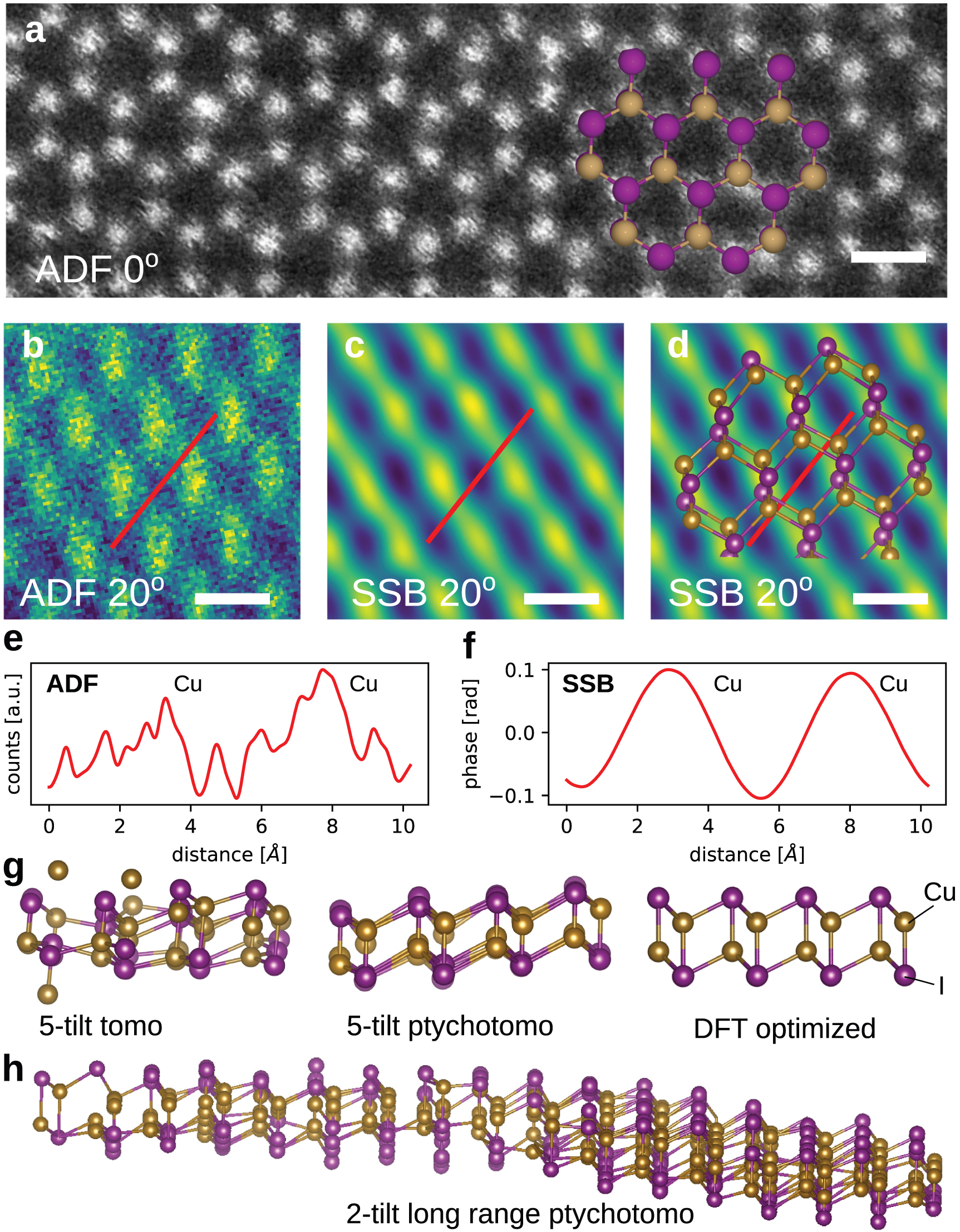
To reduce the dose imposed on the region of CuI used for the reconstruction we performed the few tilt series in a previously unirradiated region. We first acquired a series of 10 scans at zero tilt angle with a 2 µs dwell time and a dose of 
 Å−2 per scan. The simultaneous recording of ADF and 4D STEM data at this speed was made possible by our event driven Timepix3 detector [20, 25]. Importantly, the rapid scan speed greatly facilitates the low dose operation and greatly reduces the effects of drift in each scan. We build up signal by summing the drift corrected scans to obtain ADF and SSB images at
 Å−2 with next to no motion blur.
To obtain the full 3D configuration, we use data from the same region at specimen tilts of  ,
,  ,
,  , and
, and  again using drift corrected series of ten 2 µs dwell time
 Å−2 scans. At this dose it is not possible to clearly determine the positions of the Cu atoms in the tilted projections from the ADF images alone. The high atomic number of iodine conceals the lighter Cu atoms in the ADF images as shown in figure 2(b). The 3D structure thus cannot be accurately determined from the ADF images alone. Indeed, even at very high electron doses and utilising greater numbers of tilt angles the ADF images alone were not sufficient. supplementary figure 9 shows the reconstruction resulting from using ADF imaging only with five projections and relatively high dose of
 Å−2 per projection. It is evident that the Cu atoms are reconstructed with much less accuracy and precision, despite increasing the dose by approximately two orders of magnitude.
The ptychography provides a much stronger signal from which the projected positions of all the atoms can be more reliably extracted as seen in figure 2(c). The optimised model is overlaid on the same SSB image in figure 2(d), illustrating how the tilt shifts the projected positions of the atoms laterally. Despite the signal from the Cu atoms not being fully separated from that of the I in the images, the well resolved elongated shape of the tilted columns is nonetheless sufficient for the few tilt algorithm because it maximises the correlation between the simulated and experimental images, which does not require the atoms to be individually resolved. However the strength of the signal from the atoms is paramount. Line traces from along the red lines in figure 2(b) and c are shown in e and f. The strong smooth signal from the SSB ptychography is far superior for fitting atomic positions to than the noisy ADF image, and allows the algorithm to correctly identify the projected positions of even partially overlapping atoms.
The enormous benefit provided by the ptychographic phase image for few tilt reconstruction is demonstrated by comparing the models produced by the algorithm using five tilts with and without it to a model relaxed by density functional theory (DFT). These are shown viewed from the same angle in figure 2(g). Analysis of the z-heights output by the few tilt ptychotomography shows standard deviations of 12.8 pm and 14.2 pm for iodine and copper respectively and is visually clearly in line with the DFT. Because of the weak Cu signal, the ADF only reconstruction is far more disordered, with standard deviations of 32.3 pm and 80.2 pm for iodine and copper. See supplementary figure 5 for further comparison. Interestingly, the precision of the results is still greater with both ADF and ptychographic signals than using only the ptychography which produced precisions of 22.7 pm and 34.5 pm for iodine and copper, indicating that the additional information from the ADF is very useful even if it is noisy, in addition to simply distinguishing the elements. Thus, there remains significant utility in obtaining the simultaneous ADF signal at each tilt angle, as is very easy to do in focused probe ptychography.
Several factors likely contribute to the experimental precisions including residual non-linear drift, scan distortions, the finite accuracy of the tilting holder and even out-of-plane atomic vibrations. However the standard deviations reported above do not take into account the possibility that the structure might actually be curved, and the DFT modelling assumed a flat structure. Figure 2(h) shows an example of a reconstruction from a significantly wider area where the 2D CuI flake is indeed not perfectly flat, but rather substantially deformed. We were only able to collect data from two tilts before the area contaminated, again illustrating the utility of few tilt methods, particularly as the precision is already sufficient to detect the curvature. This can be directly detected in the tilted projection, where the curvature leads to a slight distortion in the lattice (see supplementary figure 6). There are various possible reasons for the curvature of 2D CuI such as the deformation of the encapsulating graphene layers, strain, contamination, and defects in the structure, none of which are captured in the small pristine model used by the DFT. In this example, we attribute the curvature to a small pore nearby, but capturing such deviations from the ideal structures assumed by DFT can be crucial to understanding emergent materials properties.
We emphasise that the signal from the bilayer graphene is too low to reliably retract. In fact, the graphene and any layer of contamination contributes rather by weakening the contrast of the CuI lattice. Even if all contamination is removed, a much higher dose than what we used is required in order to resolve the graphene lattice in the heterostructure. This is illustrated in supplementary figure 10 with simulated Gr-CuI-Gr SSB ptychography data at an electron dose of 
 Å−2 and a Gaussian blur of 1 Å to account for source size broadening. As can be seen, the graphene lattice is hidden in the stronger contribution from the CuI and leads to a slight broadening of the CuI lattice which is also seen experimentally (compare supplementary figure 8).
4. Discussion and outlook
We have developed and demonstrated a new few-tilt tomographic approach that combines ptychography with Z-contrast imaging to greatly enhance our ability to solve the 3D structure of 2D materials. The method works as long as the positions of all atoms can be tracked in all tilts, even if they are not fully resolved. The greatly expanded ability of simultaneous ptychography and ADF imaging to detect and distinguish all the atoms greatly benefits tomography in general, and the few-tilt approach is optimal for general 2D materials systems, for which 3D analysis is increasingly vital and currently very challenging. Most future 2D materials are predicted to be structurally complex [21], and we anticipate this approach, as illustrated with our two tilt analysis of curvature in CuI, to precisely reveal the true 3D structure of defected, undulating, and stacked 2D materials systems which have so far been out of reach for both experimental and theoretical methods. In addition systems composed of atomically thin 2D layers encapsulating intercalated atomic species [26, 27] can be fully characterized by this method.
5. Methods
5.1. Optimization
In detail, the correlation function to be maximized is

where the sum runs over all N probe positions in the scan, and  and
and  are the intensities of the ith pixel of the experimental data and the numerical simulation of the imaging method m (ADF or SSB) from a view V, respectively.
  and
and  are the corresponding mean values of the experimental and the simulated images, respectively and
  and
and  are the corresponding standard deviations of the experimental and simulated images, respectively. This function is maximised based on quadratic interpolation: Here, the gradients in each direction are calculated by a finite difference method and the minimum of a quadratic fit is estimated and used as the next iteration value. The whole
  can be interpreted as the sum of the correlation of each image input to the algorithm.
5.2. Electron microscopy
µs dwell time electron ptychography was conducted using a fast, event-driven Timepix3 [20, 25, 28] camera in a probe-corrected FEI Themis Z instrument with a probe convergence angle of 30 mrad and a beam current of 1 pA at 60 kV acceleration voltage. Ten scans of  probe positions were acquired sequentially at each tilt angle (
 and
and  ) with a dwell time of 2 µs. All ten data sets were processed with the SSB method and the final images were aligned and averaged using non-rigid registration. The algorithms for the SSB and the 3D reconstruction written in python can be found on gitlab [29]. The ADF images where simultaneously aquired with an detector angle between 80 and 200 mrad.
5.3. STEM simulations
STEM image multislice simulations were carried out using the PyQSTEM Package [30] using a 60 kV accelerating voltage, a convergence angle of 30 mrad and a probe step size of 18 pm. Three slices were used for the normal incident image, and up to 30 slices for the tilted structures. Thermal vibrations and the finite source size are taken into account with a Gaussian broadening of 1 Å During the optimisation procedure, simulations using the convolution method were used for its computationally efficiency [31]. The accuracy of this method is discussed in the supplementary information.
Acknowledgments
We acknowledge funding from the European Research Council (ERC) via grant number 802123-HDEM (C H and T J P) and FWO Project G013122N 'Advancing 4D STEM for atomic scale structure property correlation in 2D materials' (C H). K M acknowledges the Austrian Science Fund (FWF) (Project No. P35912) and support from Emil Aaltonen Foundation. V S was supported by the FWF (Project No. I2344-N36), the Slovak Research and Development Agency (APVV-16-0319), the project CEMEA of the Slovak Academy of Sciences, ITMS project code 313021T081 of the Research & Innovation Operational Programme and from the V4-Japan Joint Research Program (BGapEng). Danubia NanoTech s.r.o. has received funding from the European Union's Horizon 2020 research and innovation programme under Grant Agreement No 101008099 (CompSafeNano) and also thanks Mr Kamil Bernáth for his support.
Data availability statement
All data that support the findings of this study are included within the article (and any supplementary files).
Code and data availability
The raw data used for figures 1 and 2 as well as the 3D models are all available on reasonable request to the corresponding author. The ptychotomography code is available for download at https://gitlab.com/christoph_hofer/stem3dopt.
Supplementary data (9.4 MB PDF)