
Abstract
This paper benchmarks various epitaxial growth schemes based on n-type group-IV materials as viable source/drain candidates for Ge nMOS devices. Si:P grown at low temperature on Ge, gives an active carrier concentration as high as 3.5 × 1020 cm−3 and a contact resistivity down to 7.5 × 10⁻⁹ Ω.cm2. However, Si:P growth is highly defective due to large lattice mismatch between Si and Ge. Within the material stacks assessed, one option for Ge nMOS source/drain stressors would be to stack Si:P, deposited at contact level, on top of a selectively grown n-SiyGe1−x−ySnx at source/drain level, in line with the concept of Si passivation of n-Ge surfaces to achieve low contact resistivities as reported in literature (Martens et al. 2011 Appl. Phys. Lett., 98, 013 504). The saturation in active carrier concentration with increasing P (or As)-doping is the major bottleneck in achieving low contact resistivities for as-grown Ge or SiyGe1−x−ySnx. We focus on understanding various dopant deactivation mechanisms in P-doped Ge and Ge1−xSnx alloys. First principles simulation results suggest that P deactivation in Ge and Ge1−xSnx can be explained both by P-clustering and donor-vacancy complexes. Positron annihilation spectroscopy analysis, suggests that dopant deactivation in P-doped Ge and Ge1−xSnx is primarily due to the formation of Pn-V and SnmPn-V clusters.
Export citation and abstract BibTeX RIS

This is an open access article distributed under the terms of the Creative Commons Attribution 4.0 License (CC BY, http://creativecommons.org/licenses/by/4.0/), which permits unrestricted reuse of the work in any medium, provided the original work is properly cited.
The continuous downscaling of MOS devices goes together with changes in device architectures and demands for the implementation of new materials. The increase in contact resistivity (ρc) due to the decrease in source/drain (S/D) contact area is one of the major scaling issues and limits device performance.1 S/D stressors with high dopant activation are required to achieve low series resistance (between the metal contact to S/D and the S/D to channel interfaces). For Ge nMOS devices, one of the simplest choices is to use highly phosphorus (P)-doped Ge as the S/D material. However, the formation of dopant-vacancy (V) clusters in epitaxial Ge contributes significantly to the dopant deactivation, which limits the interest for this material.2
One of the methods to boost the active carrier concentration in Ge is to move the growth process away from thermal equilibrium conditions, e.g. by growing the material at low temperature using higher order precursors.3 However, such growth methods are often non-selective in nature. On the other hand, point-defect engineering approaches supported by density functional theory (DFT) calculations, suggest that the codoping with Sn could help in achieving enhanced phosphorus activation in Ge, as Sn can act as a trap for vacancies.4,5 However, Ge alloying with Sn introduces an unwanted compressive strain, detrimental for the n-Ge FinFETs. On the other hand, adding both Si and Sn to Ge allows to tune the S/D lattice parameter and transfer the preferred tensile stress to the Ge-channel. Besides a high dopant activation and the correct strain type, additional requirements for Ge nMOS S/D stressors are the possibility for conformal doping (i.e. ion-implant free), low thermal budget processing and selective growth toward oxide and nitride surfaces present on devices.
In this work, we compare various n-type (P or As doped) S/D candidates for Ge nMOS devices. One of these options is the introduction of highly P-doped Si because high dopant activation levels can be achieved in Si.6,7 A high temperature variant of a selective Si:P grown on Si substrate using SiH2Cl2 at 675 °C, gives an active carrier concentration and Hall mobility value close to 2 × 1020 cm−3 and 55 cm2 Vs−1, respectively.6,7 On the other hand, the low temperature version of Si:P grown on Si using Si3H8 at 450 °C provides active doping levels as high as 7 × 1020 cm−3 and Hall mobilities close to 35 cm2 Vs−1.8 A lower thermal budget, the correct strain type (i.e. tensile strain) and the high active carrier concentration make the Si3H8-based Si:P process an obvious choice for both Si and Ge nMOS S/D. It must be noted that although, the in − situ P-doped Si grown with Si3H8 at low temperature and directly on Ge, provides the highest active carrier concentration (3.5 × 1020 cm−3) and the lowest ρc values (7.5 × 10⁻⁹ Ω.cm2), the Si:P layers still cannot be implemented at S/D level in n-Ge FinFET devices due to the non-selective nature of the growth process. The implementation of a cyclic deposition and etch (CDE) approach using Cl2 gas as an etchant, which is specially required for low thermal budget processes since the conventional HCl etching does not work9, results in a low etching selectivity. The etching process fails to remove the amorphous Si:P from oxide or nitride surfaces with high etch rates and simultaneously preserve the crystalline material (i.e. Si:P grown on patterned Ge fins) with as low as possible etch rates. Furthermore, any exposure of the Ge underneath the Si:P during the etch process results in a complete removal of patterned Ge fins. This result is attributed to the aggressive etching of Ge as compared to Si while using Cl2 as an etchant gas.9
Meanwhile, other S/D materials such as n-Ge, n-Ge1−xSnx, n-SiyGe1−x−ySnx can be grown selectively without the need for CDE approach, but the amount of active dopants in the as-grown layers are limited to the mid 1019 cm−3 range.10 Consequently, the lowest contact resistivity values achievable with these materials are limited to ∼10−5–10−6 Ω.cm2. Therefore, none of the studied materials alone could fulfill the requirements for Ge nMOS S/D stressors. Hence, one of the viable option for n-Ge S/D FinFET device is apparently the combination of n-SiyGe1−x−ySnx at S/D level and a Si:P liner at the contact level (Fig. 1). These results are in line with the concept of Si passivation of n-Ge surfaces to achieve low contact resistivity as proposed by Martens et al.11 Recently, Jeon et al.12,13 demonstrated that heavy Sb-doping of Ge results in active carrier concentrations above 1 × 1020 cm−3 without the need for any post − epi activation anneals. The ρc values down to 10−9 Ω.cm2 were extracted using circular transmission line model (CTLM) measurements for Sb-doped Ge layers. The encouraging results for highly conductive Ge:Sb layers definitely make them attractive option for Ge nMOS S/D. However, it must be noted that CTLM measurements have a limited resolution and sensitivity for the extraction of ρc values below 10−8 Ω.cm2. Therefore, standard CTLM measurements need to be combined with either refined transmission line model (RTLM) or the Multi-Ring CTLM (MR-CTLM) measurements for an accurate determination of contact resistivities below 10−8 Ω.cm2 (Ref. 14).

Figure 1. Cross-section schematics of a n-Ge FinFET device.
Download figure:
Standard image High-resolution imageThe saturation in active carrier concentration with increasing P (As)-doping for as-grown pure Ge films or SiyGe1−x−ySnx alloys is one of the major hindrances to achieve low contact resistivity, besides the need for a lower Schottky barrier height at the metal/ semiconductor interface. E.g. the degree of dopant deactivation in Ge and Si films with the highest P concentration of 1.1 × 1020 cm−3 and 1.6 × 1021 cm−3 as we achieved in our previous studies is as high as 75% and 78%, respectively.2,10 The aim of the current manuscript is to get fundamental insights into P deactivation in epitaxial Ge and the impact of Sn-doping on dopant activation in Ge. The manifestation of As-vacancy clusters in As-doped Ge1−xSnx will be discussed in Ref. 15. The microstructural analysis behind the evolution of strain and the conductivity in Si:P films are discussed in detail in Refs. 6, 7 and 16.
The structure of the current manuscript is as follows, we will first benchmark the different materials by comparing the maximum achieved active carrier concentration and the lowest contact resistivities as extracted from micro-Hall effect (MHE) and MR-CTLM measurements, respectively. Next, we focus on the atomic interactions between the P–P, the Sn–Sn and the P, Sn with vacancies using first principles simulations. The dominating open-volume defects in Ge:P and Ge1−xSnx layers have been characterized using Positron Annihilation Spectroscopy (PAS) measurements. Results from the PAS measurements are corroborated with positron modeling using two-component density functional theory (TCDFT) to identify the type of dominant open-volume defect (i.e. mono- or di-vacancy) and its chemical environment.
Experimental and Computational Details
Growth and characterization details
The n-Ge, n-Ge1−xSnx, n-SiyGe1−x−ySnx (either lattice-matched or tensile strained with respect to Ge), and the Si:P layers were epitaxially grown by chemical vapor deposition (CVD) on blanket Ge Virtual Substrates (VSs) using a 300 mm production compatible epi tool (ASM Intrepid XPTM). The n-Ge, n-Ge1−xSnx, n-SiyGe1−x−ySnx layers with x, y ≤ 0.08 were grown at 440 °C, 315 °C and 400 °C, respectively, using conventional gas precursors (GeH4, SiH4, SnCl4, and PH3 or AsH3). Whereas, the Si:P layers were grown at 450 °C using Si3H8. The resistivity, the active carrier concentration and the Hall mobilities for as-grown layers were extracted using MHE measurements.17 A Hall scattering factor of 1 has been assumed in this study. The Sn percentage in Ge1−xSnx layers was measured by Rutherford Backscattering Spectroscopy (RBS). The Si and Sn percentage in SiyGe1−x−ySnx and the total P and As concentrations in each layer were obtained from Secondary Ion Mass Spectrometry (SIMS) measurements. Contact resistivities were extracted from the MR-CTLM structures as shown in Fig. 2 (adapted from Ref. 14) using the fabrication scheme described in Fig. 3. For each material, the growth conditions providing the highest active carrier concentration, the lowest resistivity and a thickness of ∼50 nm were used for the MR-CTLM measurements.

Figure 2. Schematic top view and the cross-sectional view along AA' of a MR-CTLM structure with 10 rings (Fig. adapted from Ref. 14). The SMetal (10 μm) and the SElectrode (0.35 to 10 μm) stand for the width of each metal ring and the electrode spacing, respectively.
Download figure:
Standard image High-resolution image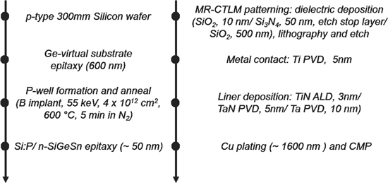
Figure 3. Process flow for the fabrication of MR-CTLM structures used for contact resistivity extraction.
Download figure:
Standard image High-resolution imageComputational details
First principles simulations were carried out in a cubic 216 Ge atoms supercell using Vienna ab initio Simulation Package (VASP) combined with the projector augmented wave (PAW) method.18–21 The electron exchange and correlation were described by two different methods i.e. standard generalized gradient approximation (GGA)/Perdew-Burke-Ernzerhof (PBE) functional and Heyd-Scuseria-Ernzerhof (HSE06) range-separated hybrid functional.22–24 We will demonstrate that the choice of electron exchange and correlation functional is critical to understand the stability of the dopant-dopant and the dopant-vacancy clusters. A 350 eV kinetic energy cutoff and the Γ point sampling of the Brillouin zone were used for both methods. The atomic positions were relaxed until forces on each atom were below 1 × 10⁻³ eV Å−1. Our previous work in Refs. 2 and 25 was limited to understanding the dopant-vacancy interactions. In this work, we extend our study not only to describe the sensitivity of different electron exchange and correlation functionals but also to understand the atomic interactions among substitutional P, Sn and the possibility of P- and Sn-clustering along with occurrence of dopant-vacancy clusters in Ge. In addition, the energetic cost to incorporate various dopant-dopant and dopant-vacancy clusters will be benchmarked, which have been missing so far.
The positron states and the annihilation characteristics for different defect complexes were modeled using local-density approximation.26 We assume that the electron density is not affected by the presence of positron and use a so-called "conventional-scheme" within the zero-positron-density limit of the TCDFT.26 The repulsive forces of the localized positrons on the ions were taken into account and the Doppler spectra were calculated using PAW all-electron wavefunctions and the state dependent scheme for annihilating electron-positron pairs.27–29 The computed spectra were convoluted with the experimentally determined detector resolution before comparison with the experimental results.
PAS characterization details
The size and the chemical environment of dominating open-volume defects in pure Ge and Ge1−xSnx layers with different P-doping levels were studied using positron annihilation spectroscopy measurements. The conventional line shape parameters, the S and the W were used to describe the annihilation spectrum. The integration windows for the S and the W parameters were set at  a.u. and
  a.u., respectively, where
  is the Doppler shift in terms of momentum and a.u. stands for the atomic units. The depth profiling was done with Doppler Broadening Spectroscopy (DOBS) using mono-energetic positrons (0.5–25 keV) obtained from a low-energy positron beam. The momentum density of annihilating electron-positron pairs was studied using coincidence Doppler Broadening Spectroscopy (CDOBS). The special feature of CDOBS measurements is the significantly reduced peak-to-background ratio especially at high momenta. This is important since, the annihilation spectrum at high momenta is dominated by positrons annihilating with core electrons. Thanks to the reduced background, slight changes in core electrons contribution around the annihilation site can be detected.30 E.g. in case of mono-vacancy defects in Ge, any variation in the number of P atoms around the mono-vacancy, when the Ge atoms are replaced by P atoms, is reflected in a difference in the number of core electrons (i.e. the 3d shell of Ge is missing). The reduced probability of positrons annihilating with the core electrons indeed leads to changes in annihilation spectrum and this in-turn allows to determine the chemical environment around the dominating open-volume defect.
Electrical Properties of n-Ge, n-Ge1−xSnx, n-SiyGe1−x−ySnx, and Si:P Layers
The electrical properties of n-Ge, n-Ge1−xSnx, n-SiyGe1−x−ySnx, and the Si:P layers with the highest active carrier concentrations achieved in this study are summarized in Table I. The highest dopant activation which we achieved for P-doped Ge layers using selective process conditions with GeH4 at 440 °C, is limited to 3.7 × 1019 cm−3 in agreement with the previous studies.3 For higher P concentrations in Ge (∼1 × 1020 cm−3), the degree of dopant deactivation is as high as 75% (Fig. 4a). In the following sections, using DFT calculations and the PAS measurements, we will discuss the P deactivation in Ge due to the formation of Pn-V clusters. We will show that there are at-least 3 P atoms attached to the mono-vacancy sized open-volume defects for epitaxial Ge with P-doping concentrations above 1 × 1020 cm−3.
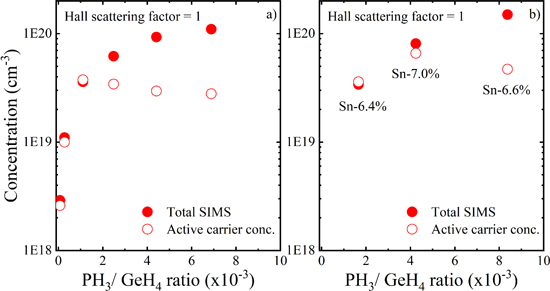
Figure 4. The total P concentration (measured by SIMS) and the active carrier concentration (extracted from μHall measurements) as function of PH3 to GeH4 mass-flow ratios for (a) epitaxial Ge and (b) Ge1−xSnx films grown at 440 °C and 315 °C, respectively. Only the PH3 flow was varied to obtain different P concentrations. Figures adapted from Refs. 2 and 25, with the permission of AIP Publishing.
Download figure:
Standard image High-resolution imageTable I.
Summary of material properties of the layers studied in this work. The electron mobility (μe), electron concentration (n) and resistivity (ρMHE)were obtained from MHE measurements. The resistivities,  and ρCTLM and contact resistivity, ρc as extracted from micro four-point probe and CTLM measurements (at end of process), respectively, and the total n-dopant concentration from SIMS measurements for n-Ge, n-Ge1−xSnx and n-SiyGe1−x−ySnx and Si:P layers with highest active carrier concentration as achieved for as-grown layers.
| μe | n | ρMHE |

|
ρCTLM | ρc | SIMS total | Selective | |
|---|---|---|---|---|---|---|---|---|
| S/D material | (cm2.V−1.s−1) | (cm−3) | (mΩ.cm) | (mΩ.cm) | (mΩ.cm) | (Ω.cm2) | (cm−3) | |
| Ge:P | 237 | 3.7 × 10¹⁹ | 0.7 | 0.7 | 0.8 | 5.6 × 10⁻⁶ | 3.6 × 10¹⁹ | Yes |
| Ge0.93Sn0.07:P | 152 | 6.6 × 10¹⁹ | 0.6 | 0.6 | 1.4 | 1.5 × 10⁻⁵ | 8.1 × 10¹⁹ | Yes |
| Si0.08Ge0.90Sn0.02:Pa) | 118 | 6.5 × 10¹⁹ | 0.8 | 0.8 | 0.8 | 1.9 × 10⁻⁶ | 7.6 × 10¹⁹ | Yes |
| Ge0.94Sn0.06:As | 138 | 8.8 × 10¹⁹ | 0.6 | 0.6 | 0.9 | 1.5 × 10⁻⁶ | 2.6 × 10²⁰ | Yes |
| SiyGe1−x−ySnx:Asb) | 79 | 8.1 × 10¹⁹ | 0.9 | 0.9 | 1.0 | 7.0 × 10⁻⁷ | — | Yes |
| Si:P | 8 | 3.5 × 10²⁰ | 2.3 | 2.3 | 1.8 | 7.5 × 10⁻⁹ | 1.6 × 10²¹ | No |
| Si:P on Ge:Pc) | — | — | — | — | — | 1.3 × 10⁻⁸ | — | No/ Yes |
| Si:P on Si0.08Ge0.90Sn0.02:Pc) | — | — | — | — | — | 1.1 × 10⁻⁸ | — | No/ Yes |
a)Tensile strained to Ge, confirmed by Reciprocal Space Mapping. b)Lattice-matched to Ge, confirmed by Reciprocal Space Mapping. SIMS measurements not available to verify the Si, Sn and total As concentrations. c)Individual conductivity of bi-layers not measurable from Hall measurements. Si:P layers are too thin for SIMS characterization.
A higher active carrier concentration (6.6 × 1019 cm−3) can be achieved when growing Ge0.93Sn0.07:P layers. However, the improvement in the activation cannot be attributed to the Sn alloying but is solely an effect of the reduced growth temperature. Indeed, similar active doping levels can be reached in Ge:P layers when grown at a similar temperature and using higher order precursors.3 Hence, there is no significant effect of Sn alloying on improving the P activation in Ge. For instance, Ge0.93Sn0.07 layer with a P concentration of 1.5 × 1020 cm−3, the degree of dopant deactivation is also as high as 70% (Fig. 4b).
Similar active dopant concentrations (6.5 × 1019 cm−3) were obtained for P-doped Si0.08Ge0.90Sn0.02 layers. The following Sections provide detailed insights into the interaction of Sn, P and mono-vacancies (the dominant open-volume defect) in Ge. DFT calculations indicate that Sn does not have the desired effect of trapping vacancies, as the binding energies for Sn-V pairs are clearly higher than for complexes involving dopants (i.e. P atoms).25 On the other hand, both experimental and the computational PAS results indicate that Sn does have an impact on the annihilation state of the positrons, indicating the presence of Sn around the mono-vacancy sized open-defects in Ge1−xSnx layers.
For the As-doped Ge0.94Sn0.06 and SiyGe1−x−ySnx (lattice-matched to Ge) layers, slightly higher dopant activations were obtained using identical growth conditions, except for the doping source (Table I).
The ρc values extracted from the Ti/Ge:P and the Ti/Ge0.93Sn0.07:P stacks were limited to 5.6 × 10⁻⁶ and 1.5 × 10⁻⁵ Ω.cm2, respectively, despite the as-grown Ge0.93Sn0.07:P layer did exhibit a slightly higher active carrier concentrations than the Ge:P layer. The comparison between  (measured on as-grown layers by the micro four-point probe technique) and ρCTLM values (extracted from CTLM measurements after the processing) suggest a degradation in material quality during the post − epi CTLM processing for both As and P-doped Ge1−xSnx layers (Table I). On the other hand, the Ti/n-SiyGe1−x−ySnx stacks, with a relatively low Sn concentration (x ≤ 2 at%) do not show such a degradation and provide lower ρc values with respect to the Ti/n-Ge1−xSnx contacts (Table I). This indeed indicates a better thermal stability of the Ti/n-SiyGe1−x−ySnx stacks and a more suitable compatibility with the final process in a n-Ge FinFET device flow. One possible reason for the high contact resistivities as obtained for relatively Sn-rich Ti/n-Ge1−xSnx contacts could be instabilities in the layer composition and strain relaxation induced during post − epi CTLM processing. The maximum temperature applied in our post − epi CTLM processing is during the deposition of the dielectric stack at 400 °C (Fig. 3). However, recent studies in literature report that undoped Ge1−xSnx layers with Sn concentrations up to 6 at% and a thicknesses of 40 nm, which are close to the Sn content and the thicknesses used in our CTLM studies, are thermally stable for annealing temperatures up to 500 °C and for annealing times as long as 30 min.31,32 No evident changes in the surface morphology, the lattice parameter and the layer composition as function of annealing temperatures between 300 °C to 500 °C for the annealed Ge1−xSnx films were observed in comparison to as-grown layers.32 Therefore, the exact mechanism resulting in high ρc values as obtained for the Ti/n-Ge1−xSnxcontacts in comparison to the Ti/n-SiyGe1−x−ySnx stacks is not yet fully understood.
The Ge:P, n-Ge1−xSnx, and n-SiyGe1−x−ySnx layers can be selectively grown, e.g. in n-Ge FinFET S/D areas of device patterned wafers. However, the materials are limited in terms of maximum active doping concentration, which is crucial to obtain low ρc values. In addition, n-Ge1−xSnx layers provide the wrong strain type for Ge channel n-FET devices. Lower ρc values down to 7.5 × 10⁻⁹ Ω.cm2 were achieved for the Si:P layers grown on Ge using Si3H8 at 450 °C. Unfortunately, the Si:P layers with the highest active doping concentration cannot be grown selectively. As discussed in the introduction section, the CDE approach to selectively grow the Si:P layers on patterned Ge fins results in a low selectivity during the etching steps. Figure 5a shows a cross-section scanning electron microscopy (SEM) image for a conformal deposition of Si:P layer grown using Si3H8 on the patterned Ge fins and on the isolating oxide surface. Different process conditions with varying deposition and etch times failed to obtain selectively grown Si:P in the open areas (i.e. on the patterned Ge fins) and simultaneously remove amorphous Si:P grown on top of oxide or nitride surfaces. Furthermore, any exposure of the Ge under the crystalline Si:P during the etching process results in a complete removal of the Ge fins as seen in Fig. 5b. This behavior is due to the aggressive etch rates of Ge in comparison to Si when using Cl2 as etchant gas.9

Figure 5. Cross-section SEM view for conformal Si:P deposition on the patterned Ge fins and the isolating SiO2 (left). Both Si:P (amorphous and crystalline) and the Ge fins are etched away after Cl2 etching step (right).
Download figure:
Standard image High-resolution imageNone of the studied materials alone could fulfill all Ge nMOS S/D requirements. The newly evaluated n-Ge1−xSnx and the n-SiyGe1−x−ySnx layers (despite relatively low resistivities values as compared to Si:P layers) could not provide  values below 1 × 10⁻⁷ Ω.cm2. An alternative solution for Ge nMOS devices would be to stack materials in order to combine the advantage of selective area deposition for n-Ge or n-SiyGe1−x−ySnx layers and the low contact resistivity from non-selective deposition of the Si:P layers. The Si:P-containing stacks enabled low ρc in combination with Ti, with a minimum ρc values approaching ∼1 × 10⁻⁸ Ω.cm2 for Si:P on Ge:P or on Si0.08Ge0.90Sn0.02:P, without any post − epi anneal (Table I). Hence, the most favorable choice for the n-Ge FinFET devices is a combination of Si:P as liner material at contact level on top of selectively grown n-SiyGe1−x−ySnx at S/D level (Fig. 1).
We benchmark our contact resistivity data with the lowest reported values in literature for n-Ge contacts (Fig. 6).13,33–39 Yu et al.38 demonstrated a ρc value of 5.5 × 10⁻⁸ Ω.cm2 for thin Si:P layer grown on top of P-doped Ge. Subsequent post metal annealing of Ti/Si:P/Ge:P contacts at 475 °C for 1 min resulted in a further reduction of ρc down to 1.4 × 10⁻⁸ Ω.cm2. As-grown Si:P cap/ Ge:P or SiyGe1−x−ySnx:P stacks considered in this study resulted in similar ρc values (i.e. ∼1 × 10⁻⁸ Ω.cm2). The consecutive post metal anneals could help in further reducing the ρc values below 1 × 10⁻⁸ Ω.cm2. Recently, Dal et al.39 reported a ρc value as low as 1.6 × 10⁻⁹ Ω.cm2 using in − situ doped and laser annealed multilayer epitaxial stacks on n-Ge. However, no precise information is available on the materials used in these stacks. As previously discussed in the introduction section, Jeon et al.13 recently reported ρc values as low as ∼7 × 10⁻¹⁰ Ω.cm2 extracted using CTLM measurements on Sb-doped Ge layers. Although, the CTLM method alone used in the study is not accurate enough to reliably extract ρc values below 1 × 10⁻⁸ Ω.cm2, still the high dopant activation achieved in Ge:Sb layers makes them promising candidate for Ge nMOS S/D.

Figure 6. Contact resistivity benchmark for n-Ge contacts.13,33–39 "This work" shows the contact resistivity for the stacks which can be integrated in Ge nMOS device flow. The ρc values in Ref. 13 were extracted using large CTLM structures with electrode spacing >5 μm.
Download figure:
Standard image High-resolution imageMicrostructural Analysis of Ge:P and Ge1−xSnx:P
We studied the atomic interactions of substitutional P and Sn atoms and the formation of Pn-V, Snm-V and SnmPn-V complexes in epitaxially grown Ge:P and Ge1−xSnx:P films. The probability of P and Sn clustering (Pn and Snm, respectively) was investigated using first principles simulations by evaluating the energetic driving forces for the coexistence of P–P or Sn–Sn pairs at different atomic substitutional sites in the Ge lattice, starting from a conformation where the atoms lie as first nearest neighbors (1nn) and evolving toward larger separations. We also determined the role of vacancies toward the formation of Pn-V, Snm-V and SnmPn-V clusters and their impact on the dopant activation in Ge and Ge1−xSnx layers. In what follows, we will first discuss the P–P and Sn–Sn interactions in a defect free Ge lattice. Later, we will discuss the local arrangement attained by P and Sn atoms in the presence of a vacancy in the Ge lattice. As discussed earlier in indtroduction section, the idea of co-doping of Ge:P with Sn is motivated by the fact that Sn being larger atom can act as a trap for vacancies and can help to boost the active carrier concentration. On the other hand, the addition of Si to Ge1−xSnx:P is to tune the lattice parameter and to compensate for the unwanted compressive strain which is detrimental for n-Ge FinFETs. Therefore, the microstructural analysis in this work has been restricted to understand the vacancy trapping efficiency of Sn in Ge:P and has not been extended to SiyGe1−x−ySnx:P.
P clustering in Ge
The systems were modeled using a supercell made of 216 Ge atoms, in which the positions of 2 P atoms were systematically varied to scan all possible atomic configurations, placing the P atoms at different radial distances from each other (ranging up to ∼8.5 Å). The total energies for the different configurations were then obtained by relaxing both the atomic coordinates and the lattice parameters. The obtained energy values were compared with the energy of the reference system for which the P–P pairs were set farthest apart from each other. Figure 7a reports the change in total energy with respect to this reference system for the most stable conformations containing 2 P atoms. Calculations were done using the standard GGA/PBE and the hybrid, HSE06 exchange-correlation functionals.22–24
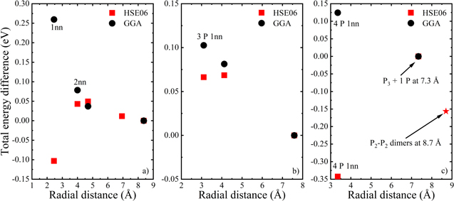
Figure 7. Evolution of the energy difference with respect to the "isolated" dopant case for a substitutional scenario where (a) 2 P atoms, (b) 3 P atoms, (c) 4 P atoms are located at different radial distances from each other in the Ge lattice. The starting configurations for (a), (b) and (c) were single isolated P atom, 2 P atoms and 3 P atoms as first nearest neighbors, respectively. The radial distances for subsequent addition of each P were calculated from the centroid of existing P atoms. Calculations were done using the standard GGA/PBE and the hybrid HSE06 exchange-correlation functional.
Download figure:
Standard image High-resolution imageAt this stage, it is interesting to note that the P–P interaction as described in literature is based on a standard GGA/PBE functional.40 It is well established that the classical GGA/PBE exchange-correlation functional describes Ge as a metallic system.41,42 This pathological behavior can be corrected using different first-order techniques, namely by using either a GGA+U approach, as implemented in Ref. 42, or a hybrid exchange-correlation treatment with the HSE06 functional.23,24 In this communication, we employ the HSE06 technique to study the dopant-dopant and the dopant-defect interactions in Ge and benchmark it against a standard GGA/PBE approach.
Based on the GGA/PBE calculations, one would conclude that the concomitant existence of 2 P atoms in their immediate vicinity maximizes the difference in total energy due to their Columbic repulsions (Fig. 7a). Following this driving force, the total energy of the system is reduced with the increase in distance between the P atoms. On the other hand, hybrid calculations based on HSE06 predict that the formation of a P–P dimer (i.e. 2 P atoms lying as first nearest neighbors) leads to the most stable configuration, which suggest that P clustering can lead to the deactivation of the dopants in Ge. So far, we have been considering only 2 P atoms in a 216 atoms Ge supercell, which corresponds to a doping concentration of 0.92%. It however must be noted that a doping concentration of 0.92% already exceeds the solid solubility of P in Ge (0.16%).43 This implies that there is a high probability for the occurrence of P–P dimers for these P-doping levels, where the active carrier concentration starts to decrease/saturate in comparison to the total P concentration in the epitaxial Ge layers. To understand the local atomic arrangement adopted in the presence of even higher concentrations, we evaluated the formation of P clusters with more than 2 atoms. The inclusion of the 3rd P atom was started from the most stable relaxed geometry obtained for 2 P atoms in dimer configuration (i.e. first nearest neighbor configuration with the lowest energy as suggested by hybrid calculations). In such a situation, the system attains its minimum energy configuration when the 3rd P atom is placed far away from the existing P–P dimer. This result was obtained for both the GGA/PBE and HSE06 calculations (Fig. 7b).
Regardless of the concentration, and for any subsequent addition of P atoms, the GGA/PBE calculations predict that the lately added P atom should lie as far as possible from the existing P atoms. However, the description obtained by HSE06 calculations leads to a different insight. The minimum energy for the system with an even number of P atoms occurs, when the P atoms are present as 1nn, as shown in Fig. 7c for the case of 4 P atoms in the Ge lattice. In this configuration, the 4th P atom was added at 3.3 and 7.3 Å from the centroid of 3 P atoms as 1nn. We also checked the scenario in which the initial configuration is chosen as being the most stable conformation in the case of 3 P atoms (i.e. P–P dimer + 1 P atom at 7.6 Å). In this situation, the most stable configuration occurs when the newly added P atom forms a dimer with the existing isolated P atom (i.e. P2-P2 dimers at 8.7 Å in Fig. 7c). The configuration P3 + 1 P at 7.3 Å was chosen as isolated/ reference system in Fig. 7c.
The question which arises at this level is, the reason for which the electrostatic interaction between the P atoms arranged as 1nn would be underestimated using GGA. A part of the answer can be found in the tendency of GGA to promote an over delocalization of the wavefunction of the valence electrons. This is reflected in Fig. 8 by the signature of the partial density of states (PDOS) for 2 P atoms in 1nn configurations (i.e. P–P dimers). The band energies in the horizontal axis are shifted with respect to the Fermi energy (i.e. 0 eV represents the Fermi-level). As depicted in Fig. 8a, there is underestimation/ no opening of the bandgap, when GGA is used as exchange-correlational functional, which minimizes the energy difference between the bonding and anti-bonding orbitals in Ge. The consequence of this artefact (i.e. the bandgap underestimation), leads to an increase in occupancy of the valence electrons in the anti-bonding orbitals. The enhanced electronic population in the anti-bonding orbitals increases the energy of the system. On the other hand, the bandgap opening resulting from the improved treatment of the Hartree-Fock exchange the HSE06 exchange-correlation functional enhances the energy difference between the bonding and anti-bonding orbital states (Fig. 8b). Consequently, lesser anti-bonding states are available to promote the delocalization of the wavefunction of the valence electrons. The resulting decreased (increased) electronic population in the anti-bonding (bonding) orbitals stabilizes the system.
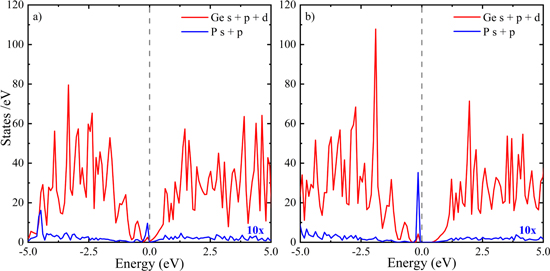
Figure 8. The partial density of states for Ge (red, s, p and d orbitals) and P (blue, s and p orbitals) atoms for P–P dimers in a Ge lattice calculated using (a) GGA and (b) HSE06 hybrid functional. A 2 × 2 × 2 Γ centered k-mesh was used to calculate the partial density of states. The PDOS for P atoms has been multiplied by factor 10 for better visualization. The band energies in the horizontal axis are shifted with respect to the Fermi energy (i.e. 0 eV represents the Fermi-level).
Download figure:
Standard image High-resolution imageIn order to obtain a detailed description of the electronic population in bonding and anti-bonding orbitals, together with the nature of the bonds involved (i.e. single (σ) or double (π) bond) between Ge-Ge, Ge-P and P–P, a natural bond orbital (NBO) analysis was performed using the VASP compatible periodic NBO software developed by Dunnington et al.44 in combination with correlation-consistent polarized triple zeta (cc-pVTZ) basis sets 45. For a detailed explanation on the NBO analysis, the reader is referred to Ref. 44.
Table II lists the resulting average electronic population in various natural bond orbitals when 2 P atoms are arranged as 1nn in Ge using the GGA and HSE06 exchange-correlational functionals. Clearly, the HSE06 description leads to a electron occupancy that decreases in the Ge-P  anti-bonding orbitals or vice-versa, increases in the Ge-P σ bonding orbitals. The lowering in the electronic population of Ge-P
  orbitals stabilizes the system more significantly with the HSE06 functional as compared to the GGA case. Furthermore, it is interesting to note that P atoms are only three-fold coordinated and form σ bond only with the nearest neighbor Ge atoms. The P atoms do not share the electrons between each other and exist as lone pairs (LP). However, the HSE06 functional increases the electronic population of the lone pairs by the reduction of electron delocalization in the anti-bonding states. As a result, the electronic signature of the LP appears within the bandgap in the HSE06 calculations (see sharp blue peak near the Fermi-level for P PDOS in Fig. 8b). The enhanced electrostatic interaction between the P atoms for the HSE06 functional is reflected by the variation in bond lengths. Figure 9 illustrates the changes in the bond lengths for P–P dimers and for the nearest neighbor Ge atoms after relaxation using the GGA and HSE06 exchange-correlation functionals. The distance between the 2 P atoms with HSE06 is set to 2.906 Å in comparison to 2.712 Å for the GGA simulations. This, in-turn, leads to a contraction of the Ge-P bonds (2.345 Å) for HSE06 in comparison (2.389 Å) to the GGA simulations. On the other hand, when 2 P atoms are placed at ∼8.5 Å apart from each other (i.e. in an "isolated" scenario), the P atoms remain four-fold coordinated to Ge. This results in an increase of the Ge-P bond lengths (∼2.430 Å) and in electronic population of the Ge-P
  orbitals as the contribution of the exchange energy vanishes at long ranges.
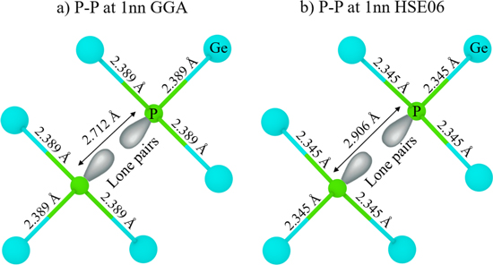
Figure 9. The variation in bond lengths for P–P dimers and nearest neighbor Ge atoms at the end of geometry relaxation as calculated using (a) GGA and (b) HSE06 hybrid functional. The Ge and the P atoms are shown in cyan and green, respectively. The gray lobes on P atoms represent the lone pairs (LP).
Download figure:
Standard image High-resolution imageTable II. The NBO analysis for P–P dimers in a Ge lattice using the standard GGA/PBE and the hybrid, HSE06 exchange-correlation functionals.
| NBOs | Occupancy GGA | Occupancy HSE06 |
|---|---|---|
| Ge-P σ | 1.856 | 1.907 |
Ge-P 
|
0.158 | 0.098 |
| Ge-Ge σ | 1.885 | 1.899 |
Ge-Ge 
|
0.089 | 0.071 |
| P LP(1) | 1.664 | 1.759 |
| P LP(2) | 1.664 | 1.759 |
Sn clustering in Ge
The random nature of the Ge1−xSnx alloy is evident from Fig. 10. It is found that the difference in total energy for the Sn–Sn configurations at different radial distances with respect to the most isolated case, i.e. with a Sn pair at 8.3 Å, lies below the thermal energy accessible at 300 K (i.e. kbT = 25 meV). This holds true, when the Sn atoms occupy atomic positions separated by at-least 4 Å apart from each other. Furthermore, similar trends were obtained for the GGA/PBE and the HSE06 calculations. Note that the configuration is assumed to be stable whenever the difference in total energy between the chosen system and the reference one is below or equal to the thermal energy at 300 K.
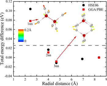
Figure 10. Evolution of the total energy difference with respect to an "isolated" system with Sn atoms lying at 8.3 Å apart from each other, for 2 Sn atoms located at different radial distances, calculated using standard GGA/PBE and hybrid HSE06 functional. For all configurations with at-least 4 Å separation between 2 Sn atoms, the energy difference lies below the thermal energy at 300 K (gray dotted line). The Figs. in the insets show strain vectors for the Sn–Sn pair at 1nn and 3nn configurations. Sn atoms arranged in 3nn configuration result in a minimum bond-bending distortion. The color bars show the magnitudes of the bond distortions with respect to pure Ge.
Download figure:
Standard image High-resolution imageAlbeit, all configurations are energetically favorable for Sn–Sn pairs positioned from 2nn onwards, it is found that the Sn–Sn pairs remain bound for certain separations. This effect is purely elastic in origin, and was also reported for the Si:C compounds by Rücker et al.46 It turns out that there is a local minimum for the relaxed 3nn configuration, when the Sn–Sn couple is set at opposite sides of the hexagonal coordination ring of Ge. This is due to a non-overlap of the strain vectors as illustrated in the inset of Fig. 10. Along these axes, the configuration results in minimum bond-bending distortions. Whereas, the overlap of strain vectors at 1nn (and for the other nearest neighbor distances) leads to strong bond-bending distortions and results in an increase in the energy for this given conformation. It must however be noted that the minimum energy configuration found for the third nearest neighbor coordination of the Sn–Sn pair is not as distinct as for the case of the complementary C-C pair in Si. The 3nn C-C pair in Si is more strongly bound as reflected by an energy difference of −0.14 eV.46
For higher Sn concentrations and irrespective of the computational approach used (i.e. GGA/PBE or HSE06), we obtained a similar trend as in the case of 2 Sn atoms in the Ge lattice. The atomic structure has the tendency to adopt a random distribution for their positions, as long as they lie at-least 2nn apart from the other Sn sites. Our findings that 2 Sn atoms can coexist as 2nn onwards, are in line with the random distribution of Ge1−xSnx alloys evidenced by Extended X-ray Absorption Fine Structure (EXAFS) results from Gencarelli et al.47
Affinity of P and Sn toward vacancies
So far, we considered atomic interactions of extrinsic species at substitutional sites within the body of the defect-free Ge lattice. The situation alters when a vacancy (i.e. a missing Ge atom) is added to the system. In this case, the energy of the different configurations (i.e. Pn-V and Snm-V) is the lowest when either the Sn or P atom is placed as a 1nn with respect to the position of the vacancy. Similarly, when both Sn and P atoms are present together in the Ge lattice with vacancies, the minimum energy configuration occurs when both Sn and P decorate the vacancies as first nearest neighbors. It must be noted that the P atoms around the E-centers (i.e. dopant-vacancy clusters) remain electrically in-active. They do not contribute to the electrical conduction in Ge or Ge1−xSnx layers.48
Until now, the energetic landscape for all possible conformations of the interacting species e.g. interactions between P (or Sn) atoms and between a P (or Sn) atom and a vacancy were mapped in order to identify the minimum energy configurations. The energetic cost to constitute different defect structures are illustrated by calculating their formation enthalpies ( ) according to Eq. 1, adapted from Ref. 49:

where EDefect is the total energy of the supercell containing the defect. EGe is the total energy of the host Ge crystal without any defect. nD (D = P, Sn ...) and nGe are the number of the dopant atoms added and the number of Ge atoms removed from the system, respectively. μD and μGe are the chemical potentials of the dopant and Ge atoms with respect to the elemental solid.
Figure 11 shows the ΔHf values for the minimum energy configurations of Pn clusters. The increasing ΔHf values with the accumulation of more P atoms in Pn clusters clearly demonstrates that their evolution becomes energetically costly. On the contrary, the decreasing ΔHf values of Pn-V clusters with increasing P concentration suggests that the P atoms are incorporated together with vacancy. However, if this hypothesis persists, the concentration of open-volume defects should either be negligible or at-least, less than the total P concentration at low P-doping levels and should increase eventually for higher P concentrations in experimentally grown Ge layers. We will demonstrate later using PAS measurements that the concentration of open-volume defects remains indeed constant in Ge for P-doping levels going from 2.9 × 1018 cm−3 to 3.6 × 1019 cm−3. For P concentrations above 3.6 × 1019 cm−3, not only the concentration of open-volume defects, but also the number of P atoms present as 1nn around them, increase with P-doping.
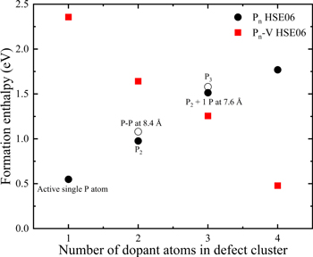
Figure 11. Benchmark of the formation enthalpies calculated using the HSE06 hybrid functional for the conformation of Pn, and Pn-V complexes with different number of P atoms in the defect cluster.
Download figure:
Standard image High-resolution imageUntil now, we have discussed two possible scenarios which can cause dopant deactivation in P-doped Ge, namely the P clustering and the formation of Pn-V clusters. The first principles simulation results discussed in Fig. 11 predict the manifestation of Pn-V clusters as the most dominating mechanism to kick-in at high P concentrations causing severe dopant deactivation in Ge. Therefore, point-defect engineering strategies are required to hinder the formation of large Pn-V clusters. The idea of codoping of Ge:P with Sn was motivated by the possibility that the passivation of vacancies by Sn atoms could enhance the dopant activation in Ge. If Sn atoms trap free vacancies, less sites around the vacancies would be available for P atoms. As a result, the P atoms would remain four-fold coordinated which would result in a higher P-doping activation in Ge1−xSnx, as compared to Ge.4,5 However, the HSE06 simulations do not support this idea. According to our simulation results, it is highly unlikely that the Snm-V clusters are formed because of their too high formation enthalpies in comparison to the Pn-V clusters. Figure 12 shows the calculated formation enthalpies using Eq. 1 for various Snm-V, SnmPnV and Pn-V clusters. It is evident from the calculated ΔHf values that the conformation of Pn-V clusters involve minimal energetic cost followed by the SnmPnV and the Snm-V complexes for same number of alien atoms around the mono-vacancy. The rapid shift of the ΔHf values for the SnmPnV clusters toward the Pn-V complexes with increase in number of P atoms around the vacancy implies that the former are most likely to occur subsequent to the formation of Pn-V clusters. Moreover, the SnmPnV complexes are expected to be P-rich with increasing P-doing in Ge1−xSnx alloys. It must be noted that any P atoms present in form of SnmPnV complexes also remains deactivated in the Ge lattice. This simulation results are in line with the electrical results and give a qualitative explanation for the fact that experimentally extracted highest electron concentrations are very similar for Ge:P and Ge1−xSnx:P (Fig. 4). Meaning, there is hardly any impact of Sn-doping on boosting the dopant activation in P-doped Ge. This leads us to the question, what is the dominant defect type and its chemical environment in epitaxially grown Ge or Ge1−xSnx films? To answer these questions, we will now switch to the PAS analysis on Ge and Ge1−xSnx layers.

Figure 12. Benchmark of the formation enthalpies for various Snm-V, SnmPnV and Pn-V clusters with different number of P and Sn atoms in the defect clusters. The ΔHf values were calculated using HSE06 hybrid functional.
Download figure:
Standard image High-resolution imageChemical Environment of Dominating Open-volume Defects in Epitaxial Ge and Ge1−xSnx Films using PAS Measurements
According to first principles simulations, dopant-vacancy defects are the dominating defects in Ge as well as in Ge1−xSnx, as the formation enthalpies values of larger clusters are lower compared to the  values of dopant-dopant clusters (Figs. 11 and 12). To validate the presence of the most dominating open-volume defects in as-grown P-doped Ge and Ge1−xSnx layers and their dependence on P-doping, we have performed DOBS and CDOBS measurements on all samples reported in Fig. 4. The studied samples include P-doped Ge and Ge1−xSnx grown on top of 600 nm Ge-VS. The thicknesses of the Ge:P and Ge1−xSnx:P layers were ∼100 nm and ∼80 nm, respectively.2,25 To interpret the CDOBS spectra obtained from the P-doped Ge and Ge1−xSnx layers, we calculated the momentum densities of the Pn-V and the SnmPn-V clusters in the Ge lattice. A similar experimental PAS analysis was performed on As-doped Ge1−xSnx layers. Both Ge1−xSnx:P and Ge1−xSnx:As show similar characteristics, the addition of Sn fails to hinder the formation of dopant-vacancy clusters, which in-turn causes severe dopant deactivation in both Ge1−xSnx:P and Ge1−xSnx:As. There are at-least 3 dopant atoms present around the mono-vacancy at doping concentrations above 1 × 1020 cm−3. Therefore, we keep our discussions restricted to Ge1−xSnx:P layers in this work, whereas the PAS analysis on Ge1−xSnx:As will be discussed in Ref. 15.
Evolution of Pn-V clusters in Ge
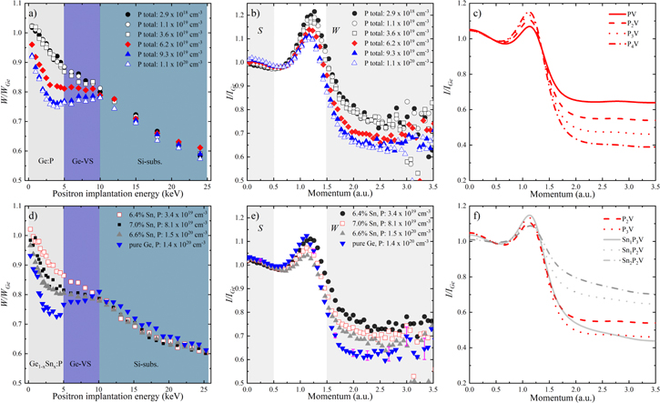
The upper panel of Fig. 13 shows the normalized DOBS (W parameters as function of positron implantation energy, Fig. 13a) and the CDOBS (experimental momentum distributions in form of ratio plots scaled to defect-free Ge-reference, Fig. 13b) measurement results obtained on P-doped epitaxial Ge films. The different shaded regions in Fig. 13a indicate the energy intervals where measured W parameters correspond mainly to the positrons annihilating in the top Ge:P layer (0.5-5 keV), the Ge-VS (5-10 keV) and the silicon substrate (above 10 keV), respectively. The steep decay in W parameters throughout the Ge epi-layers indicate that the as-grown layers are full of open-volume defects. Furthermore, the decrease in W parameters with increasing P-doping as seen for P concentrations above 3.6 × 1019 cm−3, signifies an increased concentration of open-volume defects in the Ge films. Interestingly, no change in the W parameters has been observed for the P-doping ranging from 2.9 × 10¹⁸ to 3.6 × 1019 cm−3. This means that the concentration of dominant open-volume defect remains constant in this doping range. For higher P concentrations, the decrease in measured W parameters suggests that the dopant incorporation in Ge goes together with the incorporation of vacancies. This is line with our theoretical results presented in Fig. 11, suggesting the lower formation enthalpies for the larger Pn-V (n > 2) clusters at high P concentrations.
Figure 13. (a), (d) The normalized W parameters vs positron implantation energy, (b), (e) measured momentum distributions at a positron energy of 4.5 keV, and (c), (f) the calculated momentum distributions of the Pn-V and the SnmPn-V clusters for the Ge (upper panel) and the Ge1−xSnx (lower panel) films with different P concentrations. The shaded regions in (a) and (d) indicate the energy intervals where the measured W parameters correspond mainly to the positrons annihilating in the top Ge:P or the Ge1−xSnx:P layer (0.5–5 keV), the Ge-VS (5–10 keV) and the silicon substrate (above 10 keV). The experimental and calculated momentum distributions in (b), (e) and (c), (f) are scaled to a defect-free Ge-reference sample and a bulk 216 atoms Ge supercell, respectively. Figures were adapted from our previous work in Refs. 2 and 25, with the permission of AIP Publishing.
Download figure:
Standard image High-resolution image
The identification of the dominant defect-type and its chemical environment is determined from the CDOBS measurements. These measurements were done at a positron incident energy of 4.5 keV. At this energy nearly all positrons annihilate in the top Ge:P layer. The momentum distributions for the different Ge films as function of P-doping are shown in Fig. 13b. The measured intensities in the peak region (1 < p < 1.5 a.u.) confirm the presence of mono-vacancy defects. Typically, lower intensities are observed in the peak region for the larger open-volume defects.50 The positron annihilation at high momenta (p > 1.5 a.u.) is mainly dominated by the positron annihilating with the 3d core electrons of Ge.30 The decrease in intensity at high momenta with increasing P-doping signifies that the chemical environment around the mono-vacancy is changed. This decrease in intensity is due to the increased number of P atoms around the mono-vacancies. This reduces the annihilation probability of the positrons with core electrons at high momenta, since P atoms do not have 3d shell electrons. The calculated momentum distributions for Pn-V clusters in Ge as shown in Fig. 13c confirm the observed trend of decreasing intensity at high momenta. However, it must be noted that in Fig. 13c only single defect types (e.g. P1-V or P2-V) are modeled under periodic boundary conditions. On the other hand, the experimental spectra shown in Fig. 13b are superpositions of positrons annihilating in Pn-V clusters within the Ge films with different n-values. By comparing Figs. 13b and 13c, it can be concluded that the open-volume defects (i.e. mono-vacancies) which dominate the measured annihilation spectra for Ge layers are passivated by at-least 2 P atoms for P-doping ranging from 3.2 × 10¹⁹ to 6 × 1019 cm−3 and by at-least 3 P atoms in case of P-doping concentrations above 9 × 1019 cm−3.
Evolution of SnmPn-V clusters in Ge1−xSnx
The lower panel of Fig. 13 shows PAS results as obtained on the Ge1−xSnx:P layers. The DOBS measurement results in Fig. 13d show similar characteristics for the W parameters as function of P-doping in the Ge1−xSnx layers as observed in case of Ge:P layers (i.e. the concentration of open-volume defects increases with P-doping). Figure 13d includes a comparison of a Ge:P and a Ge1−xSnx layers which contains nearly the same electron carrier concentration (5.7 × 1019 cm−3 vs 4.7 × 1019 cm−3) and nearly the same total P concentration (1.4 × 1020 cm−3 vs 1.5 × 1020 cm−3). This allows to study the impact of Sn-doping on the positron trapping. In this case, the Ge sample was grown using Ge2H6 at a similar temperature (320 °C) as used to grow the Ge1−xSnx layers (315 °C). Apparently, the Ge1−xSnx layer exhibits higher W parameter. This increase in the W parameter is attributed to the reduced size of the dominating open-volume defects in the Ge1−xSnx layers due to presence of Sn atoms around them.
In our previous work (Ref. 25), we have demonstrated that the relaxation effects for the atoms present around the vacancy play an important role in positron trapping. Since the Sn atoms relax in the inward direction with respect to the vacancy, the size of the open-volume defect in case of Snm-V clusters becomes considerably smaller, which prevents the positron trapping. On the other hand, for the SnmPn-V clusters where the alien atoms around the open-volume defect relax in both outward (P atoms) and the inward direction (Sn atoms), in this case the positron remains trapped within the open-volume if there are at-least 2 P atoms around the mono-vacancy.25
The CDOBS measurements in Fig. 13e show momentum distributions for positrons annihilating in the Ge1−xSnx layers with different P concentrations. The incident positron energy for CDOBS measurements on Ge1−xSnx layers was the same as in the case of Ge:P layers (i.e. 4.5 keV). The intensities measured in the peak region (1 < p < 1.5 a.u.) once again confirm that both as-grown Ge:P and the Ge1−xSnx:P layers have the same type of dominant open-volume defects (i.e. mono-vacancies). The decreased intensity at high momenta with increasing P-doping clearly reflects the increase in number of P atoms around the mono-vacancy. The mono-vacancy sized defect complexes which dominate the measured annihilation spectrum are passivated by at-least 2 P atoms in case of a P concentration of 3.4 × 1019 cm−3 and by at-least 3 P atoms for P concentrations above 8.1 × 1019 cm−3. The result obtained on the pure Ge sample, which is included in Fig. 13e, clearly exhibits a lower intensity at high momenta as compared to the Ge1−xSnx layer with a similar P concentration, although the dominating defect cluster in both samples has at-least 3 P atoms present around the mono-vacancy. This higher intensity obtained for the Ge1−xSnx layer is attributed to the presence of Sn atoms around the vacancy along with the P atoms. The calculated momentum distribution for different SnmPn-V clusters are shown in Fig. 13f. The presence of a Sn atom around a mono-vacancy, e.g. in case of Sn1P3-V complex leads to slight increase in intensity at high momenta as compared to P3-V cluster. On the other hand, a significant increase in intensity is observed for Sn1P2-V and Sn2P2-V complexes with respect to a P2-V cluster. The experimental spectra shown in Fig. 13e for the Ge1−xSnx layers with different P concentrations are superpositions of positrons annihilating in the Pn-V and the SnmPn-V clusters. Therefore, we conclude that there is at-least 1 Sn atom around the mono-vacancy for the Ge1−xSnx sample with highest P concentration (i.e. 1.5 × 1020 cm−3). Although the dominant defect in the Ge1−xSnx layer has at-least 3 P atoms around the vacancy, there are still SnmPn-V clusters with at-least 1 Sn atom present around them which contributes toward the measured annihilation which ultimately results in an increased intensity at high momenta for the Ge1−xSnx layer with same P concentration as in the Ge:P layer.
Conclusions
We studied the maximum active dopant concentration and the minimum possible contact resistivities achievable for various epitaxial growth schemes based on n-type group-IV materials available as options for n-Ge S/D stressors. None of the studied materials alone could fulfill all necessary requirements of Ge nMOS S/D layers. The n-Ge or n-SiyGe1−x−ySnx layers can be grown selectively in S/D areas. However, they exhibit limited doping activations and high contact resistivities (Table I). Despite the higher doping concentration and the lower contact resistivity which were achieved for as-grown Si:P, the implementation of this material in n-Ge FinFET device remains challenging due to the non-selective nature of the growth process. In addition, Si:P layers grown on Ge are highly defective due to the large lattice mismatch with respect to the underlying Ge-VS. Therefore, we propose the use of Si:P as liner material to achieve the low contact resistivity in combination with n-SiyGe1−x−ySnx as S/D material to obtain the lowest resistance path between the S/D and the Ge-channel (Fig. 1).
The possible dopant deactivation mechanisms in the P-doped Ge were studied using first principles simulations. Advanced DFT calculations using HSE06 hybrid functional suggest that P-clustering (e.g. formation of P–P dimers) along with the formation of Pn-V complexes can explain the limited doping activation in Ge. At high P concentrations (>1 × 1020 cm−3), the formation of Pn-V complexes is energetically more favorable than the formation of Pn clusters. The existence of Pn-V complexes was confirmed using experimental PAS studies on P-doped Ge layers. For P concentrations between 2.9 × 10¹⁸–3.6 × 1019 cm−3, pure substitutional P incorporation is favored and full dopant activation is achieved. PAS measurements also indicate that the concentration of open-volume defects remain similar (reflected by comparable W parameters, Fig. 13a) for this P-doping range. For higher P concentrations (>3.6 × 1019 cm−3), the dopant incorporation in Ge goes together with the incorporation of vacancies. There are 2 to 4 P atoms around the mono-vacancy sized open-volume defects. These results are in line with our theoretical calculations since the formation of P3-V and P4-V clusters is predicted to be thermodynamically favorable at high P concentrations in Ge.
The assessed point-defect engineering strategy, namely the codoping of Ge:P with Sn as trap for vacancies, has no impact on the dopant activation in Ge. This is primarily due to the higher attraction of vacancies toward the P atoms as compared to the Sn atoms due to the lower formation enthalpies of the Pn-V clusters as compared to the Snm-V complexes. PAS measurements on Ge:P and Ge1−xSnx layers show similar trends concerning the increase in number of P atoms around the mono-vacancy with increasing P concentration. The W parameters are higher for the Ge1−xSnx layer as compared to the Ge layer with the same P concentration. This indeed signifies that the annihilation state is different in the Ge1−xSnx and reflects to the presence of Sn at first nearest neighbor sites around the open-volume defects.25 This increase in the W parameters is attributed to the reduced size of the open-volume defect caused by the inward relaxation of Sn atoms with respect to vacancies. The increased intensity at high momenta for the Ge1−xSnx layer with the same P concentration as in the Ge:P layer indicates the presence of SnmPn-V clusters with at-least 1 Sn around the mono-vacancy (Figs. 13e and 13f). On the other hand, for Ge1−xSnx layers with P concentrations above 8 × 1019 cm−3, there are at-least 3 P atoms around the mono-vacancy for the most dominant defect. This indeed is a formidable evidence for the strong attraction of vacancies toward the P atoms as predicted by the first principles simulations and this is probably the dominant dopant deactivation mechanism in Ge as well as in Ge1−xSnx.
Acknowledgments
The imec core CMOS program members, European Commission, the TAKEMI5 ECSEL project, local authorities and the imec pilot line are acknowledged for their support. Air Liquide Advanced Materials is acknowledged for providing advanced precursor gases. A. V. acknowledges his long stay abroad grant and a grant for participation in congress abroad from the Research Foundation-Flanders (Application No. V410518N and K159219N). I. M. acknowledges financial support from Academy of Finland (Project Nos. 285 809, 293 932 and 319 178). CSC-IT Center for Science, Finland is acknowledged for providing the computational resources.