


Abstract
Dumbbell-like structures are recently found to be energetically favored in group IV two-dimensional (2D) materials, exhibiting rich physics and many interesting properties. In this paper, using first-principles calculations, we have investigated the oxidized form of the hexagonal honeycomb (ODB-h) and zigzag dumbbell silicene (ODB-z). We confirm that both oxidization processes are energetically favorable, and their phonon spectra further demonstrate the dynamic stability. Contrary to the pristine dumbbell silicene structures (PDB-h and PDB-z silicene), these oxidized products ODB-h and ODB-z silicene are both semimetals with Dirac cones at the Fermi level. The Dirac cones of ODB-h and ODB-z silicene are at the K point and between Y and Γ points respectively, possessing high Fermi velocities of 3.1 × 10⁵ m s−1 (ODB-h) and 2.9–3.4 × 10⁵ m s−1 (ODB-z). The origin of the Dirac cones is further explained by tight-binding models. The semimetallic properties of ODB-h and ODB-z are sensitive to compression due to the self-absorption effect, but quite robust against the tensile strain. These outstanding properties make oxidized dumbbell silicene a promising material for quantum computing and high-speed electronic devices.
Export citation and abstract BibTeX RIS

Original content from this work may be used under the terms of the Creative Commons Attribution 4.0 licence. Any further distribution of this work must maintain attribution to the author(s) and the title of the work, journal citation and DOI.
1. Introduction
Inspired by the great success of graphene [1–3], elated research has been conducted to search for monolayer mode of the same group elements. Monolayer 2D sheets of silicon, germanium, and tin, namely silicene, germanene, and stanene, have been predicted to be stable and also have recently been achieved by epitaxial growth on substrates [4–6]. A lot of attention has been paid to silicene [7–14] due to its relevance to silicon-based microelectronic industry. Unlike graphene, free-standing silicene has a low-buckled (LB) single-layer structure due to the pseudo-Jahn–Teller effect [15]. The resulting dangling bond makes silicene easily chemically functionalized by many kinds of adsorbed atoms or functional groups [16, 17], such as hydrogen [18–20], halogens [21], alkali earth, transition metals [22], oxygen [23, 24] and CH3 groups [25]. Recently, it was shown that by adsorbing Si atoms, silicene reconstructs and form dumbbell-like (DB) units [26, 27]. These DB units significantly stabilize the structure, and a series of DB silicene structures was proposed based on such DB units.
Pristine DB silicene with dumbbell units arranged in a honeycomb pattern (PDB-h) was reported to be a strain-induced quantum spin Hall (QSH) insulator [28]. Also, its allotrope with DB units arranged in a zigzag pattern (PDB-z) was demonstrated to have the lowest energy of all dumbbell silicene structures [29]. Furthermore, with the dangling bonds passivated by hydrogen atoms or by some organic clusters, functionalized DB structures have been reported to be stable and exhibiting interesting electronic properties, which has dramatically extended its possible applications [30–32]. However, in contrast to pristine and hydrogenated structures, studies of oxidization are scarce, while oxidization is very important for the application of silicon-based materials [24].
Using density functional theory (DFT), we demonstrate that O atoms can be chemically bonded to these silicon atoms on top site of PDB-h and PDB-z, leading to oxidized dumbbell silicene (labeled as ODB-h and ODB-z respectively), which have geometries similar to hydrogenated DB stanene [30]. We have investigated the structural and electronic properties along with the energetics of ODB-h and ODB-z and demonstrated their energetic and dynamic stability. More interestingly, both types of oxidized dumbbell silicene possess Dirac cones at the Fermi level. In ODB-h, Dirac cones are at the high-symmetry K point with a high Fermi velocity of 3.1 × 10⁵ m s−1. In ODB-z, Dirac cones are situated on the line between Y point and Γ point in the Brillouin zone, with an anisotropic Fermi velocity of 2.9–3.4 × 10⁵ m s−1. The analysis of the atomic orbital projected density of states (PDOS) and electron wavefunctions of the Dirac cones shows that in ODB-h and ODB-z, the pz orbitals of Si(α) and even more than px,y orbitals of oxygen atoms dominantly contribute to the Dirac cones. This conclusion is further confirmed by our tight-binding models containing only the px,y orbitals of O atoms, which well reproduces the PBE electronic band structures near the Fermi level. Moreover, we have investigated the effect of external strain on the electronic properties of ODB-h and ODB-z and found that the semi-metal property is robust against tensile strain. Finally, with the spin-orbital coupling (SOC) effect taken into account, nontrivial bandgaps of roughly 20 meV are opened, which shows that ODB-h and ODB-z are both topological insulators.
2. Computational details
All the calculations were performed employing the projector augmented wave (PAW) [33, 34] based density functional code VASP [35, 36]. The generalized gradient approximation in the form of Perdew, Burke, and Ernzerhof [37] (PBE) was used for the exchange-correlation potential. The energy cutoff of the plane waves was set to 600 eV. The energy precision of 10−5 eV was used for the convergence. The effect of vertical interaction was avoided by taking a vacuum of more than 20 Å. The structures were optimized using the conjugate gradient algorithm (CG) until the maximum Hellmann-Feynman force on each atom becomes smaller than 0.01 eV Å−1. The Brillouin zone (BZ) was sampled by using 11 × 11 × 1 Monkhorst–Pack grid. SOC was included in the Hamiltonian [38]. The phonon spectra were calculated using a frozen phonon approach [39] within the PHONOPY code [40].
The binding energies of O atom to DB silicene are calculated by

where E(ODB) and E(PDB) denote the energies of honeycomb or zigzag ODB silicene, and PDB silicene, E(O) denotes the energy of one isolated oxygen atom.
As the electronic bandgap in PBE calculation is underestimated, we have also used the Heyd–Scuseria–Ernzerhof (HSE) hybrid functional in the framework of HSE06 [41]. The energy cutoff of the plane waves is the same as for the PBE calculation, and the BZ was sampled by using 15 × 15 × 1 Gamma centered Monkhorst–Pack grid.
3. Results
3.1. Optimized geometries
The optimized geometry of PDB-h silicene monolayer is shown in figure 1(a). In this configuration, the Si atoms can be divided into two types, fourfold coordinated Si(α) atoms, similar to Si atoms in a bulk crystal, and threefold coordinated Si(β) atoms, similar to atoms in LB silicene. Every three Si(α) and two Si(β) atoms form one cage-like unit, and the cage-like units are arranged in a hexagonal honeycomb pattern. Our calculated lattice constant is 7.43 Å, which is in good agreement with reference [26]. The thickness of the configuration given by the distance between up-plane and down-plane Si(β) atoms is 2.71 Å.
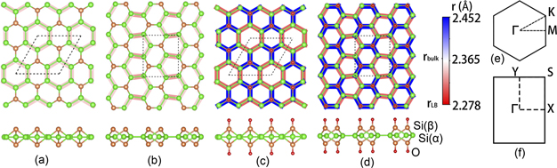
Figure 1. The top and side views of optimised geometries of PDB-h, PDB-z, ODB-h, and ODB-z shown in (a), (b), (c), and (d) respectively. The green, orange, and red balls are Si(α), Si(β), and oxygen atoms, respectively. The background color of the top views illustrates the Si–Si bond length, r. Moreover, in the color bar, the Si–Si bond length in LB silicene (rLB) and bulk silicon (rbulk) is shown for comparison. The high symmetry points at the first Brillouin zones of hexagonal honeycomb structures and zigzag structures are shown respectively in (e) and (f).
Download figure:
Standard image High-resolution imageWith all three-fold silicon atoms bonded with oxygen atoms, we get the ODB-h structure, as shown in figure 1(c). In ODB-h, not only Si(α) but also Si(β) atoms are fully coordinated. The Si–O bond length is 1.55 Å, roughly the same as that in β-cristobalite [42], and smaller than that of Si–O bond in α-quartz (1.61 Å). The lattice constant is increased to 7.49 Å, with a longer distance of 4.32 Å between two same-plane Si(β). The thickness of the monolayer characterized by the distance between up-plane and down-plane O atoms increases to 5.92 Å, in which the distance between up-plane and down-plane Si(β) atoms increases to 2.82 Å, implying stronger sp3 hybridization in Si(β).
By ab initio structure-prediction calculations using a constrained crystal-structure prediction algorithm, Borlido et al. predicted that a zigzag like DB silicene has the lowest energy among all DB silicene structures [29]. As shown in figure 1(b), PDB-z silicene is also realized with cage-like units, but the units are arranged in a zigzag pattern. According to our PBE functional calculations, the primitive cell is a rectangle, with its lattice parameter being 6.40 Å and 7.42 Å, and the area being 4.75 Å2/atom, almost the same as in PDB-h, i.e. 4.78 Å2/atom.
The oxidized form, ODB-z silicene is shown in figure 1(d). With a similar rectangular unit cell, the lattice constants are enlarged to 6.47 Å and 7.48 Å. The distance between two Si(β) layers is 2.83 Å, and the Si–O bond length is 1.55 Å, both of which are very close to that in ODB-h, implying similar hybridization mechanism in ODB-z and ODB-h silicene.
The Si-Si bond lengths are illustrated by the background colors in figures 1(a)–(d). In all the PDB and ODB structures, the bonds between two Si(α) atoms (labelled as rα,α ) are shorter than 2.365 Å, showing red colors, and the bonds between Si(α) and Si(β) atoms (labelled as rα,β ) are longer than rα,α , showing white or blue colors. Comparing the Si–Si bond lengths in pristine DB silicene and oxidized DB silicene, oxidization significantly changes the Si–Si bonds. In PDB structures, rα,α and rα,β are quite close to the Si–Si bond length in bulk silicon (rbulk). In contrast, in ODB structures, the two lengths are very different. By oxidization, rα,α is shortened to roughly 2.28 Å, close to the Si–Si bond length in LB silicene (rLB), while rα,β are increased to about 2.45 Å.
3.2. Chemical bonding and structural stability
To compare the bonding nature in PDB-h, PDB-z, ODB-h, and ODB-z, electron localization functions (ELF) are calculated and analyzed. To highlight the bonds between Si(α), Si(β) atoms, and between Si(β) and O atoms, we plot the sliced ELF contour map in the top panel of figure 2. The region with an ELF value of 1 indicates fully localized electrons, the region close to 0 is typical of a low electron density area, and the region of 0.5 is an area with a homogeneous electron gas. Interestingly, the ELF contour plots of ODB-h and ODB-z are quite similar, which implies that the bonding mechanism of ODB-h and ODB-z have no significant difference. Comparing PDB and ODB monolayers, it is found that with O atoms adsorbed, the localization of electrons inside the DB silicene layers is weakened. Compared to PDB, electrons between Si(α) and Si(β) in ODB silicene are less localised. Furthermore, in ODB, the electrons around O atoms behave mainly as a homogeneous electron gas. The binding energy of O atoms in PDB-h and PDB-z silicene is, respectively, −5.19 eV/O atom and −5.17 eV/O atom, implying that O atoms are chemisorbed on pristine DB-h and DB-z.
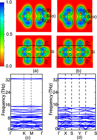
Figure 2. The top panel is the (x, y)-plane slice view of the ELF of PDB-h and ODB-h (a), PDB-z, and ODB-z (b). The bottom panel is the phonon spectrum of ODB-h (c), and ODB-z (d), respectively.
Download figure:
Standard image High-resolution imageContrary to carbon atoms, silicon atoms prefer to be fourfold co-ordinated compared to threefold co-ordination. This is seen from the relatively higher stability of pristine DB-h and DB-z compared to LB silicene. With dangling bonds filled by O atoms, the stability of ODB-h and ODB-z is quite promising. We will investigate the stability by their energetic preference, which is measured by their formation energy, and through their dynamical stability, which is confirmed by their phonon spectra.
The formation energy of oxidized DB silicene can be hinted at by the reaction: Si10 + O2 → Si10O4, in which Si10 denotes PDB silicene, O2 is oxygen gas, and Si10O4 is ODB silicene. The negative formation energy (−0.675 eV/atom for ODB-h and −0.667 eV/atom for ODB-z) implies that the reaction is exothermic. We further confirmed their dynamic stability by the phonon spectra calculated along the high symmetry directions in the first BZ, as shown in figure 2 of the bottom panel. It is observed that the phonon spectra of ODB-h and ODB-z are quite similar in the low energy part. In both cases, the optical phonon modes have a gap at around 6 THz, and most of their optical phonon modes below 7 THz are concentrated around 3.5 THz and 5 THz. There are several high energy modes (of about 34 THz) in both structures, whose eigenvectors are shown in the supplementary files (https://stacks.iop.org/NJP/23/023007/mmedia) ODBh.mp4 and ODBz.mp4, respectively [43]. The high energy modes are corresponding to the strong chemical bonds between Si and O atoms [44]. Notably, it can be seen that there are no or only tiny imaginary frequencies near the Γ point, and the structures are therefore expected to be dynamically stable.
3.3. Electronic structure
To examine the electronic structure of oxygen functionalized DB silicene, we first calculate the local DOS (LDOS) for Si(α), Si(β), and O layers. As shown in figure 3, in both ODB-h and ODB-z, pz orbital of O atoms contributes to the energy states from −3 eV to −1 eV and hybridizes strongly with pz orbitals of Si(β). Near the Fermi level px,y orbitals of O atoms significantly contribute to the electronic structure and hybridize with the p orbitals of Si(α). The strong hybridization in ODB can decrease the binding energy of O on DB silicene, and thus stabilize the structures. Interestingly, in both cases, the DOS shows a gapless electronic structure with zero DOS at the Fermi level.

Figure 3. From bottom to top panel is the LDOS projected on Si(α), Si(β), and O layers of (a) ODB-h and (b) ODB-z. PDOS of s, px,y , and pz orbitals and total DOS of corresponding layers are distinguished with yellow, blue, green lines, and orange area, respectively.
Download figure:
Standard image High-resolution imageHere, we analyze the electronic band structures of honeycomb and zigzag PDB and ODB. As shown in figure 4(a), PDB-h monolayer shows an indirect PBE bandgap of ∼0.24 eV with valence band maximum (VBM) at K point and conduction band minimum at Γ point, in agreement with the results of previous works [27, 28]. By oxidization, it is found that ODB-h is a gap-less semiconductor where VBM and CBM meeting at the K point. Near Γ point, the local valence band maximum (LVBM) and the local conduction band minimum (LCBM) are at the same place, Γ point, and LVBM degenerates with second local valence band maximum (LVBM-1), which features are also found in PDB-h. The energy difference between LVBM and LCBM at Γ point is about 0.32 eV, 0.27 eV smaller than that in PDB-h. With two bands crossing linearly at the Fermi level, the charge carriers can be characterized by massless Dirac fermions. By a linear fitting of the band structure, following

we obtain the Fermi velocity of ODB-h to be 3.1 × 10⁵ m s−1, which is comparable to those of the group IV elemental monolayers (4.7–8.5 × 10⁵ m s−1), according to the definition, the effective mass of charge carriers

equal to zero near the Fermi level. Therefore, ODB-h silicene is expected to have ultra–high carrier mobility.
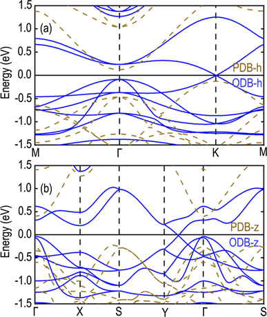
Figure 4. PBE band structure of (a) PDB-h and ODB-h, (b) PDB-z and ODB-z. The energy is set to zero at the Fermi level.
Download figure:
Standard image High-resolution imageAs shown in figure 4(b), PDB-z monolayer shows an indirect bandgap of roughly 0.62 eV with CBM both at Γ point and VBM near S point. At the Γ point, the energy level of LVBM is only 0.04 eV lower than VBM near S, which is in the correct range for applications in photovoltaics [29]. Interestingly, similar to PDB-h silicene, its oxide, ODB-h, is also a gapless semiconductor with two bands crossing linearly at the Fermi level at a point on the path between Y and Γ points. Since the Dirac cone is not situated at high symmetry points, similar to 1T-YN2 and 1T-LaN2 [45, 46], H4,4,4-graphyne [47], PAI-graphene [48], and Tungsten boride [49], the Fermi velocities are anisotropic. By a linear fitting of the two bands crossing the Dirac point, we get two different Fermi velocities for the two bands (with slopes S > 0 and S < 0) νF(S > 0) = 3.4 × 10⁵ m s−1, and νF(S < 0) = 2.9 × 10⁵ m s−1. The high Fermi velocity and massless carrier character make the ODB-h and ODB-z ideal materials for building high–speed electronic devices.
As illustrated in figure 3, for ODB-h and ODB-z, the states in the vicinity of the Fermi level are mainly from px,y orbitals of O atoms, px,y orbitals of Si(α) atoms and pz orbitals of Si(α) atoms. To reveal the relationship between electronic band structures and atomic orbitals, we have shown the projected orbitals to bands in figures 5(a) and (c), where the size of a dot demonstrates the contribution of the respective atomic orbital to the electronic bands. It is found that in ODB-h, the LVBM and LVBM-1 at Γ point are dominated by px,y orbitals of Si(α) with a little contribution by px,y orbitals of O atoms, while the VBM/CBM at K points is mainly contributed by px,y orbitals of O atoms, and pz orbitals of Si(α) atoms. Moreover, in ODB-z, px,y orbitals of Si(α) atoms mainly contribute to the bands near Γ point, while the Dirac cones are made up by px,y orbitals of O atoms and pz orbitals of Si(β) atoms. These features of the bands at K point are also demonstrated in the density profiles of VBM/CBM electronic wave functions shown in figures 5(b) and (d).
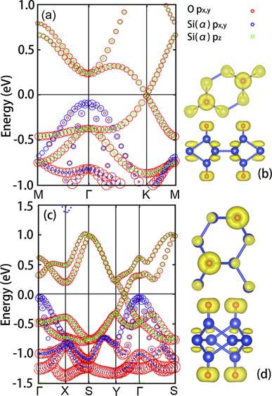
Figure 5. The orbital projected band structures of (a) ODB-h and (b) ODB-z along high symmetry path in the BZ, and the corresponding electronic wave functions of VMB/CBM (c) and (d).
Download figure:
Standard image High-resolution image3.4. Tight-binding model
To reveal the origin of the Dirac cone explicitly, tight-binding (TB) models are helpful. As illustrated in figures 5(c) and (d), both Si(α) and O atoms contribute to the Dirac cone, the electronic wave functions of O atoms are much larger than those of Si(α) atoms. By proposing simple TB models, which only include the px,y orbitals of O atoms, we are able to fit the bands near the Fermi level.
To further illustrate the origin of the Dirac points in the two monolayers, we propose two TB models involving the px and py atomic orbitals. The effective Hamiltonian is taken as in reference [50]

where  ,
,  , and
, and  represent the on-site energy, creation and annihilation operators of an electron at the α-orbital of the ith atom, respectively. The
  parameter is the nearest-neighbour hopping energy of an electron between an α-orbital of ith atom and β-orbital of jth, and α, β ∈ (px
, py
). Considering the hexagonal lattice first, we neglect the interactions between the O atoms in different z planes, because the nearest-neighbor distance in the z-direction is more than 20 Å, which is much less than that in the xy plane. We only consider the O atoms in the up/down plane, which is a graphene-like lattice. This graphene-like lattice with px,y
atomic orbitals leads to a Dirac point in the K point, which is similar to in previous investigated systems of BiX/SbX (X = H, F, Cl, Br, I) [51]. According to the TB theory, only one
parameter is the nearest-neighbour hopping energy of an electron between an α-orbital of ith atom and β-orbital of jth, and α, β ∈ (px
, py
). Considering the hexagonal lattice first, we neglect the interactions between the O atoms in different z planes, because the nearest-neighbor distance in the z-direction is more than 20 Å, which is much less than that in the xy plane. We only consider the O atoms in the up/down plane, which is a graphene-like lattice. This graphene-like lattice with px,y
atomic orbitals leads to a Dirac point in the K point, which is similar to in previous investigated systems of BiX/SbX (X = H, F, Cl, Br, I) [51]. According to the TB theory, only one  parameter should be considered, and the hopping energies can be evaluated on the basis of two parameters (Vppσ
and Vppπ
). Since all atoms are oxygen atoms, we can neglect the on-site energy difference of these atoms and set it as 0. Taking Vppσ
= 0.4 eV and Vppπ
= −0.2 eV, the band structure from TB calculation can reproduce the DFT band structures close to the Fermi level and the Dirac point in the K point (see figure S1 in the supplementary information (SI)). For the rectangular lattice, we still chose to neglect the interactions between the O atoms in different planes and set the on-site energy to zero. Different from the hexagonal lattice, there are two nearest-neighbour hopping energies, leading to four parameters (Vppσ
, Vppπ
, V'ppσ
, and V'ppπ
). Taking Vppσ
= 0.7 eV, Vppπ
= −0.3 eV, V'ppσ
= 0.0 eV and V'ppπ
= −0.2 eV, we obtained the band structure from TB calculations. The location of the Dirac point on the line from Y point to Γ is in good agreement with the result of DFT. From the above TB calculations for the two lattices, we prove that the Dirac points in the two lattices mainly originate from the px
and py
atomic orbitals of O atoms.
parameter should be considered, and the hopping energies can be evaluated on the basis of two parameters (Vppσ
and Vppπ
). Since all atoms are oxygen atoms, we can neglect the on-site energy difference of these atoms and set it as 0. Taking Vppσ
= 0.4 eV and Vppπ
= −0.2 eV, the band structure from TB calculation can reproduce the DFT band structures close to the Fermi level and the Dirac point in the K point (see figure S1 in the supplementary information (SI)). For the rectangular lattice, we still chose to neglect the interactions between the O atoms in different planes and set the on-site energy to zero. Different from the hexagonal lattice, there are two nearest-neighbour hopping energies, leading to four parameters (Vppσ
, Vppπ
, V'ppσ
, and V'ppπ
). Taking Vppσ
= 0.7 eV, Vppπ
= −0.3 eV, V'ppσ
= 0.0 eV and V'ppπ
= −0.2 eV, we obtained the band structure from TB calculations. The location of the Dirac point on the line from Y point to Γ is in good agreement with the result of DFT. From the above TB calculations for the two lattices, we prove that the Dirac points in the two lattices mainly originate from the px
and py
atomic orbitals of O atoms.
3.5. Tensile strain
External compressing/tensile strain is reported as a feasible method to tune the electronic structures of 2D materials and transform them between metal, semiconductor, and semimetal [28, 52, 53]. Here we investigate the mechanical and electronic properties of ODB-h and ODB-z under strain, which is applied by changing the lattice constant from a0 to (1 + τ)a0. Under biaxial compressing/tensile strains of −5% < τ < 10%, as shown in figures 6(a) and (b), the energy changes continuously without any abrupt changes, which indicates that no structural transition occurs. Notably, it does not mean that the two structures are dynamically stable under the strains. Due to the freedom in out-of-plane direction, two-dimensional materials are not dynamically stable under compressive strain [54]. Under tensile strain, as shown in figure S7 in the SI, ODB-h is demonstrated to be still stable when τ = 10%. In contrast, ODB-z is not dynamically stable when τ = 10%, but it is stable when τ = 8%. The structural robustness against intense strain is related to its buckling configuration, similar to the low-bucking structure of silicene.
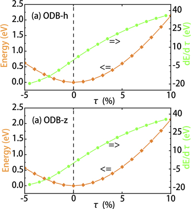
Figure 6. Energy (in orange) and energy derivative (in green) as a function of in-layer tensile strain τ. The energy is set to zero at τ = 0.
Download figure:
Standard image High-resolution imageUnder such strains, the Dirac cones near the Fermi level in ODB-h and ODB-z are always conserved. The band structure evolution is presented in the SI (figures S2 and S3). In ODB-h, under tensile strain, the Dirac cone is exactly at the Fermi level, and the bandgap at the Γ point is maintained until τ > 9%. In contrast, under compressing strain, the Dirac point moves below the Fermi level, and the bandgap at Γ point vanishes for τ < −2%, making the nanosheets behave as n-type doped. The self-doping behavior arises from the buckling structures, which is also found in LB silicene and germanene [55]. This is because the Dirac cone at K point is dominated by pz orbitals of Si(α) and px,y orbitals of O, which are not sensitive to the in-plane strains. In contrast, the LVBM and LVBM-1 at the Γ point made up of px,y orbitals of Si(α), which are affected by the change of Si-Si bond length. With similar structural features, ODB-z behaves quite similarly. Under tensile strain, ODB-z preserves the semimetallic property until 9%, while under compressing strain, the self-doping behavior makes it metallic. Overall, for τ < 9%, the semimetallic features of ODB-h and ODB-z are preserved, with the Fermi velocities changing less than 2.5%, and the insensitivity to tensile strain is advantageous for applications in complicated mechanical environments.
We have also performed band structure calculations with SOC taken into account. Considering that the Si and O are quite light, the SOC effect is generally not strong. For both ODB-h and ODB-z, with or without SOC, the band structures do not change significantly, except that SOC can introduce a bandgap of roughly 10 meV. This bandgap is much more significant than that of LB silicene, i.e. 1.55 meV [5]. The difference is due to the Dirac cone formation mechanism. In LB silicene, the Dirac cone at K point is only formed by pz orbital of Si atoms, while in ODB-h and ODB-z silicene, px,y orbitals of O atoms contribute much more than other atomic orbitals.
Since SOC opens a band gap at the Dirac cones in ODB-h and ODB-z, the topological properties are investigated. It is noteworthy that the chemical adsorption of atoms or molecules also leads to realizing topological insulators [56, 57]. As both ODB-h and ODB-z are inversion symmetric, the topological invariant Z2 can be calculated using the parity criteria method [58], which claims that the topological invariant can be determined by the parities of the time-reversal and parity invariant points in the BZ, as shown in figure 7. For 2N occupied bands, the Z2 index ν is defined by

where  is the parity eigenvalue of the 2nth occupied energy band at the time-reversal and parity invariant points Γi
. For ODB-h, δi
values of the four time-reversal invariant momenta are −1 at Γ point, and +1 at three M points. For ODB-z, the δi
values are −1 at Γ point, and +1 at X, S, and Y points. Thus the Z2 indexes of ODB-h and ODB-z are nontrivial, e.g. ν = 1, demonstrating that they are both 2D topological insulators.
is the parity eigenvalue of the 2nth occupied energy band at the time-reversal and parity invariant points Γi
. For ODB-h, δi
values of the four time-reversal invariant momenta are −1 at Γ point, and +1 at three M points. For ODB-z, the δi
values are −1 at Γ point, and +1 at X, S, and Y points. Thus the Z2 indexes of ODB-h and ODB-z are nontrivial, e.g. ν = 1, demonstrating that they are both 2D topological insulators.

Figure 7. Brillouin zone of (a) ODB-h and (b) ODB-z. b1 and b2 are the primitive reciprocal lattice vectors. The signs of δi at the time-reversal invariant momenta are labelled as +, −.
Download figure:
Standard image High-resolution image
Considering the underestimation of the bandgap in PBE calculations, we perform HSE06 calculations to examine the results. By HSE06 calculation, in both ODB-h and ODB-z, the electronic bands near the Fermi level are changed a bit: in most regions, the distance between the lowest conduction bands and highest valence bands is enlarged, while the Dirac cones are preserved. Considering the SOC effect, bandgaps of roughly 20 meV open up at the Dirac cones. These details are shown in figures S5 and S6 in the SI.
4. Conclusions
In summary, based on density functional calculations, we have investigated oxidized form of recently proposed dumbbell silicene DB-h and DB-z and have found that functionalization with O is energetically favorable. We have confirmed the dynamical stability of both oxidized products, 2D ODB-h, and ODB-z silicene by phonon calculations. Although ODB-h and ODB-z have different symmetry, both of them are found to be semimetals with Dirac cones. Also, the semimetallic property is found to be robust against tensile strain up to 9%. Furthermore, their Fermi velocities are as large as 3.1 × 10⁵ m s−1 (in ODB-h) and 2.9–3.4 × 10⁵ m s−1 (in ODB-z), which are important for application in high-speed electronic devices.
Data availability statement
The data that support the findings of this study are available upon reasonable request from the authors.
Acknowledgments
We thank Mingwen Zhao and Björn Alling for their help and useful discussions. This work is supported by the project Grant (2016-05366) and the Swedish Research Links programme Grant (2017-05447) from the Swedish Research Council, the Fonds voor Wetenschappelijk Onderzoek (FWO-Vl), and the FLAG-ERA project TRANS 2D TMD. We gratefully acknowledge supercomputing time allocation by the Swedish National Infrastructure for Computing (SNIC) and PRACE DECI-15 project DYNAMAT. Linyang Li acknowledges financial support from the National Natural Science Foundation of China (Grant No. 12004097), the Natural Science Foundation of Hebei Province (Grant No. A2020202031), and the Foundation for the Introduced Overseas Scholars of Hebei Province (Grant No. C20200313). Xin Chen thanks the China scholarship council for financial support (No. 201606220031).