


We introduce an integration ready design of metamaterial infrared absorber, highly compatible with many kinds of fabrication processes. We present the results of an exhaustive experimental characterization, including an analysis of the effects of single meta-atom geometrical parameters and collective arrangement. We confront the results with the theoretical interpretations proposed in the literature. Based on the results, we develop a set of practical design rules for metamaterial absorbers in the infrared region.
I. INTRODUCTION
Since they were first introduced by Landy et al.,1 metamaterial absorbers (MAs) have been widely studied.2 Their operation range has extended from microwaves all the way up to visible light.2–7 Their potential applications include absorption enhancing in bolometers, spectral selectivity tailoring on thermal emitters, and electromagnetic signature control.8–10
Conceptually, metamaterials are arrangements of artificial structures, identical to each other, called “meta-atoms.” Both, the meta-atom size and the characteristic distance between them, are in the subwavelength scale. The response of the metamaterial is not only due to the chemical composition of the materials it is made of but also the geometrical configuration of the meta-atoms. Although composed of discrete components, the modeling of its optical properties was usually done as homogeneous mediums with effective parameters ϵe(ω) and μe(ω).
Typically, a MA is implemented in the form of a metal-dielectric multilayer with overall thickness smaller than the operation wavelength. Some of the layers are homogeneous; some of them are periodically microstructured in the plane. Landy's original approach consists of three staked layers: an array of electric ring resonators (ERR) and an array of wires, separated by an optically thin dielectric spacer. On the other hand, contemporary designs employ a metallic ground-plane on the backside spaced from an array of metallic resonators by a dielectric layer.
At first, MAs were modeled with an effective medium theory, as was usual for metamaterials, with their effective optical properties estimated from experimental measurements of the scattering parameters. However, the authors of subsequent publications pointed out the significant fact that MAs were actually metasurfaces, highly anisotropic in the propagation direction of the light.11 Furthermore, as the operation wavelength decreased, the ground-plane backplated design was favored and scattering parameters could not be fully determined. Under this conditions, effective medium theories are not valid anymore and new ways of modeling the MAs become required.
Numerous theories have been proposed in the last years, some based on multiple reflections in the stratified media11 and others based on coupling to complex plasmonic modes.12 The applicability of each of these theories to different systems and wavelengths is still not clear.
Even though a few excellent review works on metamaterial absorbers2 describe extensively the current advances in the area and the multiple future possibilities, when it comes to start an application driven research line, where concrete guidelines are needed, not good reference can be found.
In this work, we introduce a flexible design for a metamaterial absorber operating in the thermal infrared range, which does neither require high temperature or corrosive processes nor high resolution lithography as a part of the fabrication process, hence being easily integrable in existing devices. Based on the results of the experimental characterization of the proposed design and an extensive bibliographic research, we define a body of guidelines with the hope that it would be helpful to the application-driven groups approaching the study of MA in the future.
II. REFERENCE SYSTEM
The MA design we propose as a good candidate for integration is schematized in Figure 1(a). It is a ground-plane-based design, consisting of an array of cross shaped resonators placed on top of the metallic plane, separated by a thin dielectric spacer.

Reference system. (a) Schematics of the proposed system, unit cell (bottom) and cross-section (top). Gold parts are represented in yellow and SU-8 parts in green. (b) SEM image of a finished sample.
Reference system. (a) Schematics of the proposed system, unit cell (bottom) and cross-section (top). Gold parts are represented in yellow and SU-8 parts in green. (b) SEM image of a finished sample.
The cross geometrical shape was chosen because it provides certain degree of freedom on the design and guarantees a response insensitive to polarization, without increasing the overall complexity. Using simple geometries allows the fabrication of the production samples by optical lithography, which has to be replaced by e-beam lithography or other high resolution techniques if the geometrical features get too small.
We choose the ground-plane and the metallic crosses to be made of gold, because of its good conductivity at infrared frequencies and low chemical reactivity. We selected the SU-8 photoresist as the material for the spacer. This epoxy resist has high compatibility with all kinds of microfabrication processes, because it only requires low temperature annealing for its deposition, while presenting strong chemical and thermal stability. Its capability of being UV patterneable could be useful in certain applications too.
In our study, we choose to use e-beam lithography based lift-off to fabricate the resonator array in order to take advantage of varying the geometrical parameters of the meta-atoms high precision while avoiding the effects of the spread on size and shape of the crosses. However, for application purposes, they can be easily reproduced by a much simpler and efficient optical lithography based processes.
Gold films were grown by e-beam assisted evaporation, and very thin (a few nm) Ti layers were used for adhesion purposes. The SU-8 spacer was obtained by conventional processing of a flood exposed spin-coated film of SU-8 2001 resist.13 Oxygen plasma was used to modify the surface chemistry, improving the e-beam resist adhesion after the development of the SU-8 spacer.
Figure 1(b) shows a SEM image of one of the finished samples.
III. THEORETICAL MODELLING
We are not going to present a thorough theoretical modeling but some considerations are needed to be done. There is no consensus on how ground-plane-based MAs work at infrared frequencies. Conceptually, similar structures were proposed by Nielsen et al.,12 Liu et al.,4 and Chen,11 for operation in near infrared, mid infrared, and at teraHertz frequencies, respectively. Although all the aforementioned publications claim scalability to other operating wavelengths, the interpretation offered by each one of them for the absorption mechanism differs significantly. While Liu et al. explain the absorption by classical effective medium theory, where two different resonant modes of the same structure interact with the electric and magnetic parts of the electromagnetic field of the light; the other two works acknowledge only electric mode interactions.
The proposal of Chen11 is an interference-based theory for the explanation of the response of MA operating at the microwave range. In this interpretation, the structured metallic sheet is only radiatively coupled to ground-plane, and the absorption is the result of multiple reflections in the stratified media.
On the other hand, while working on the visible and near infrared range, Nielsen et al.12 disregarded the multilayer effect and took into account the coupling between the metallic resonators and the ground-plane. They attribute the absorption to the efficient coupling of the light to gap plasmon-polariton modes resultant of the interaction between the surface plasmon modes at the interface of both metal films and the dielectric spacer.
In general, ground-plane-based metasurfaces could be modeled as multilayer resonators as is sketched in Figure 2(a).

Theoretical model. (a) Multiple reflections in the sample, where tij represents transmission coefficient, rij is the reflection coefficients, and p is the phase acquired by propagation through the spacer. (b) Equivalent system that allows us to model our design by a transfer matrix formalism, although it includes a mirror.
Theoretical model. (a) Multiple reflections in the sample, where tij represents transmission coefficient, rij is the reflection coefficients, and p is the phase acquired by propagation through the spacer. (b) Equivalent system that allows us to model our design by a transfer matrix formalism, although it includes a mirror.
Assuming small losses, so that multiple reflections can take place, the reflectance of the system should be calculated as the interference of the direct reflection and the multiple internal reflections.
Even if multilayer systems containing mirrors could not be modelled in the transfer matrix formalism,14 we can define an equivalent system that is going to bring us the right scattering coefficients. The proposed model is schematized in Figure 2(b) and is composed of five layers. The first layer stands for the crosses array, and the second one for the spacer. The third one represents the mirror and contribute with a phase shift of π, while acting as a symmetry axis for the full arrangement. So, layers 4 and 5 are the mirrored image of layers 2 and 1. The transfer matrix of the equivalent system can be written as
where is generic shape of the transfer matrix of the metallic array, is the phase shift acquired in the propagation through the spacer, and models the phase shifting function of the mirror.
The reflectance of the real system is the sum of the reflectance and transmittance channels of the equivalent system, which can be written as
where r12 and t12 are the reflection and transmission coefficients when the light crosses the resonator array from air to SU-8, t21 is the transmission coefficient for the incidence in the opposite direction, and is the phase that is acquired because the propagation through the dielectric spacer.
From this theoretical perspective, Salisbury screens,15 Nielsen's, and Chen's absorbers could be reinterpreted as different limits of the same structure.
In the case where the resonator array is purely resistive, hence the reflection and transmission coefficients are real, the first term's phase is 0, and the phase shift of the second term is acquired purely by propagation. To be able to get destructive interference, we need both terms phase to be the same, resulting in the known rule of the quarter wave thickness for the spacer.
In Chen's theory, the resonator array has complex impedance, leading to complex transmission and reflection coefficients. In this case, the phase shift is acquired partly on the reflection/transmission through the metallic array and partly on the propagation through the spacer. Therefore, under the right conditions, the spacer could be much thinner, being compensated by the phase shift in the structured metallic layer. Facing a small increment on the spacer thickness, we expect a displacement of the resonance toward longer wavelengths.11
The Nielsen's absorbers are on the other limit of possible parameters of the structure, where the phase shifts because propagation in the spacer is negligible. The metallic resonators couple to the ground-plane, and interference occurs between two modes: the light that after feeding the gap plasmon resonators is re-emitted with its phase shifted, and the light that is simply reflected by the metallic plane. In this case, as the increment in the gap size reduces the coupling between the surface plasmons in the dielectric-metal interfaces, a displacement toward smaller wavelengths is expected for thicker spacers.12
Under the strict definition of metasurfaces, the changes on the properties of the light must happen abruptly, in distances much smaller than the wavelength,16 as opposed to acquiring it by gradual accumulation during propagation. Under this point of view, only Nielsen's absorbers are “pure” metasurfaces, while Chen's structures can be regarded as “mixed” metasurfaces, as they use both resonant coupling and propagation to get the required phase shift.
IV. IMPACT OF THE GEOMETRICAL PARAMETERS OF SINGLE META-ATOMS
To characterize the response of the absorbers, we measured the reflectance of the samples by FTIR microscopy using a Microscope coupled to a Bruker™ Vertex 80v FTIR spectrometer.
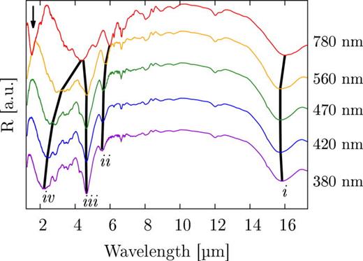
The top panel of Figure 3 shows the typical spectrum of our absorber samples, in the full wavelength range of the experimental setup used. Although the absorbers are designed to operate in the mid-infrared range, a broader characterization could bring extra information for the interpretation of the phenomena and can be useful for applications where light of multiple ranges is used. The main mode of absorption is present at a wavelength of 13.5 μm and is identified with the roman number i. Three relatively strong secondary modes at smaller wavelengths are identified with successive roman numbers. Multiple smaller resonances, typically spectrally thin, could be distinguished through all the spectrum. This minor absorptions can be attributed to the vibrational modes of the molecules that compose the dielectric spacer material.

Top frame: typical spectral response of an absorber sample. Arrows mark the more pronounced absorption modes. The main mode is labeled as (i) and secondary modes with subsequent roman numbers. Main frame: effect of the uniform scaling on the spectral response of the absorbers. In the vertical axis, the length of the crosses arms is given as a measure of the scaling. The color map corresponds to the reflectance intensity. We call the scaling of the pattern “uniform” because the parameters a/l = 1.25 and w/l = 0.25 were kept constant. The thickness of the spacer is 380 nm for this samples. The red line marks the position of the cross section of the top panel. The white line marks the linear fitting of the spectral position of the mode (i). Black arrows mark the intersection between the geometrical modes of the structure and the vibrational modes of the molecules of the material. An anti-crossing behaviour can be seen. The grey arrow marks one resonance, attributed to one vibrational mode of CO2, where no anticrossing behaviour is observed. The data of the graphic were interpolated, and the discontinuity on mode (ii) dashed behaviour is a numerical artefact.
Top frame: typical spectral response of an absorber sample. Arrows mark the more pronounced absorption modes. The main mode is labeled as (i) and secondary modes with subsequent roman numbers. Main frame: effect of the uniform scaling on the spectral response of the absorbers. In the vertical axis, the length of the crosses arms is given as a measure of the scaling. The color map corresponds to the reflectance intensity. We call the scaling of the pattern “uniform” because the parameters a/l = 1.25 and w/l = 0.25 were kept constant. The thickness of the spacer is 380 nm for this samples. The red line marks the position of the cross section of the top panel. The white line marks the linear fitting of the spectral position of the mode (i). Black arrows mark the intersection between the geometrical modes of the structure and the vibrational modes of the molecules of the material. An anti-crossing behaviour can be seen. The grey arrow marks one resonance, attributed to one vibrational mode of CO2, where no anticrossing behaviour is observed. The data of the graphic were interpolated, and the discontinuity on mode (ii) dashed behaviour is a numerical artefact.
Figure 3 (bottom panel) shows the shift on the spectral response varying scale of the crosses array. The red line marks the position of the cross-section of the top panel. The scaling was made uniformly preserving the proportionality between the size of the crosses and the array's periodicity (a/l) and the aspect ratio between the length of the arm of the crosses and its width (w/l); the thickness of the spacer was kept constant. As representative parameter, l is shown in the vertical axis. It can be seen that modes (i), (ii), and (iii) shift toward smaller wavelengths with the downscaling, while mode (iv) keeps its spectral position constant. It is important to remark that the resonance frequency shift is linear with the scaling.
The main mode can be identified as the longitudinal mode of the cross arms. The relation between resonance wavelength and arm length can be estimated by a linear fitting as , where nd is the spacer refractive index. This result implies that the field is confined under the cross and inside the gap, but discards the possibility of high confinement under Nielsen's theory. The not null y-intercept can be attributed to a small phase shift acquired on reflection at the end of the arms of the crosses. With regard to mode (iii), it is not clear if it is the first transversal mode or a higher order longitudinal mode.
The black arrows mark a few of the crossings between the resonances of the vibrational modes of the material and the geometrical modes of the structure. An anticrossing behaviour can be observed on most of them, showing strong interaction between them and field intensification in the gap. By contrast, a few modes does not show this behaviour, for example, the one present at 4.2 μm wavelength and marked with a grey arrow at the figure. They can be attributed to the vibrational modes of the surrounding gas, CO2 in this example, present in the optical path of the experiment but outside the gap of the absorber, where the field is not intensified and enhanced interaction is not expected. It is important to note that the resonance positions of the vibrational modes are not sensitive to the scaling away from the resonance wavelengths of the geometrical modes.
Figure 4 shows the effect on the spectral response of the change on the aspect ratio of the arms of the crosses. Illustratively, SEM images of single resonators are shown for certain parameters. The different geometrical modes evolve in different ways as the arms get wider. The mode (i) becomes more efficient in the absorption, but for arms too wide the absorption peak broads and shift toward longer wavelengths. By contrast, the modes (ii) and (iii) get narrower as the aspect ratio increases, and present a shift toward shorter wavelengths for the narrower arms. This makes sense if we identify the modes as first order longitudinal and transversal, as the active area increases for the longitudinal and decreases for transversal mode as aspect ratio approaches the unity. The mode (iv) is again not affected by the geometrical transformations.

Effect of the change in the aspect ratio of the arms of the crosses (w/l) on the spectral response of the absorber. SEM images of single resonators are given for certain aspect ratios for illustrative proposes. The values of the parameters l = 4 μm, a = 5 μm, and d = 380 nm were kept constant.
Effect of the change in the aspect ratio of the arms of the crosses (w/l) on the spectral response of the absorber. SEM images of single resonators are given for certain aspect ratios for illustrative proposes. The values of the parameters l = 4 μm, a = 5 μm, and d = 380 nm were kept constant.
Figure 5 shows the spectral response of samples consisting in identical arrays, but with different spacer thickness. The resonance positions are linked with black line segments. It can be seen that in the range from 380 nm to 560 nm the spectral positions of modes (i), (ii), and (iii) are not greatly affected, while the resonance of the mode (iv) systematically shifts toward longer wavelengths as the spacer gets thicker. For the sample with the thickest spacer, small shifts occur on the spectral positions of the three modes at longer wavelengths, but the shift is much bigger for the mode (iv), including the onset of a new minimum, indicated by a black arrow. Estimating the refractive index of the spacer, it is possible to show that the absorption peaks of the mode (iv) are due to a quarter wave resonance between the crosses and the ground plane.
Effect of the change of the thickness of the spacer on the spectral response. Labels mark the thickness in nm, and black segments link the position of the different modes. The values of the parameters l = 4.8 μm, a/l = 1.25, and w/l = 0.25 were kept constant.
Effect of the change of the thickness of the spacer on the spectral response. Labels mark the thickness in nm, and black segments link the position of the different modes. The values of the parameters l = 4.8 μm, a/l = 1.25, and w/l = 0.25 were kept constant.
The insensitivity to alterations on the spacer thickness suggests that the phase acquired in propagation through the gap is negligible and confirms that interaction between the superficial plasmons in the interfaces is weak. This result locates the system in the large gap limit of the Nielsen's theory and the small gap limit of Chen's theory. The shift toward longer wavelengths in thickest spacer sample indicates that the structure is entering to the regime where multiple reflections are more important.
V. IMPACT OF THE META-ATOMS ARRANGEMENT
In this section, we want to explore the role of the arrangement of the meta-atoms in the spectral response of the absorbers. It is generally accepted that there is no interaction between cells and that the response of an array is the sum of the responses of every single element. It have been shown that it is still possible to get high absorption with disordered absorbers,17 while other works claim that periodicity is essential to the absorption mechanism.
To explore the impact of a non-periodical arrangement, we designed a set of samples with different degrees of randomness in the position of the crosses. We introduced disorder in the designs by starting with a perfectly ordered sample and adding a small random gaussian distributed displacement in the crosses positions. Some SEM images of resulting samples are shown on the top part of Figure 6. The numbers in the labels are a measure of the width of the displacement distribution, corresponding a higher number to a more amorphous sample.
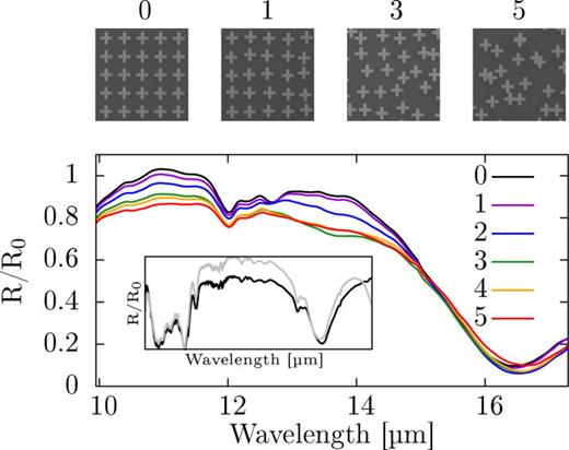
Effect of the disorder in the crystalline arrangement of the meta-atoms. Label numbers are a measure of the disorder degree. The geometrical parameters of the metaatoms are l = 5 μm, w/l = 0.25, and d = 800 nm. Inset: Spectral response of a sub-array of 5 × 5 crosses (black) and from a full sample (grey). The geometrical parameters of the metaatoms are l = 4 μm, w/l = 0.25, and d = 380 nm.
Effect of the disorder in the crystalline arrangement of the meta-atoms. Label numbers are a measure of the disorder degree. The geometrical parameters of the metaatoms are l = 5 μm, w/l = 0.25, and d = 800 nm. Inset: Spectral response of a sub-array of 5 × 5 crosses (black) and from a full sample (grey). The geometrical parameters of the metaatoms are l = 4 μm, w/l = 0.25, and d = 380 nm.
Figure 6 (bottom part) shows the spectrum of the increasingly disordered samples.
The effect of the configurational order in the main absorption peak is weak but for smaller wavelengths an increase of the reflectivity can be seen. This increment that grows even over the reference signal is more pronounced for the higher ordered samples. Discarding the possibility of near field interactions, the effect can only be attributed to interference effects.
Resonant modes of the single resonators are excited by the incident radiation, and they re-emit the energy that is not absorbed with their characteristic angular pattern. Approximating the crosses as the superposition of two perpendicular wires, we can model the emission as an array of oscillating electric dipoles. Therefore, the angular dependence of the emission of single resonators is proportional to ,18 with a maximum in the direction out of plane.
When emitters are arranged periodically, the single source emitting pattern is modulated by the array factor, as it is known from antenna theory.19 If the incidence is normal, all the resonators re-emit in phase, and the array factor can be written as
where N is the number of sources, a is the periodicity of the sources, and λ is the wavelength. So the directivity increases with the number of sources and when the periodicity a approaches λ. When the periodicity surpasses λ, higher orders appear at no normal directions and the directivity is lost.
In Figure 6, absorption happens at wavelengths where d < λ, while at smaller wavelengths d ∼ λ, the directivity increases and the measured signal with it. This sensitivity to the directivity can be expected if, during the detection process, the light fraction with the higher incidence angle is lost. In the inset of Figure 6, the spectrum of a small area of only 5 × 5 crosses is shown in black and the reflectance of the whole sample in grey. We can see that as the number of resonators decreases, the anomalous reflectance due to increment of the directionality disappears.
If interference can be used to improve reflectance, the next question that arises is: can it be used to enhance absorption? To analyse this problem, we need to remember that our theoretical model, described in Section III, was intrinsically unidimensional, being all the reflections and transmissions normal to the surface. In a metasurface with low directivity, part of the emitted light does not present the right direction and does not interfere destructively, resulting essentially in the emergence of radiative losses. Therefore, an increment in directionality by interference is expected to lead to more efficient absorbers.
The top panel of Figure 7 shows the spectral response of samples made with identical meta-atoms, but different array periodicities. Opposite to our initial expectations, any increment of the periodicity implies a drop in the absorption. This is due to the fact that a decreasing of the density implies a decrease in the number of crosses over the measurement area. As the absorption is proportional to the number of resonators, a drop in the efficiency is expected.

Effect of the periodicity of the arrays on the spectral response. Top: Reflectivity of samples with identical meta-atoms and different periodicities a/l. The geometrical parameters of the metaatoms are l = 4 μm, w/l = 0.25, and d = 800 nm. Bottom: Variation of the reflectivity of the samples with wavelength and periodicity, for a fixed number of crosses and measurement area. The geometrical parameters of the metaatoms are l = 5 μm, w/l = 0.25, and d = 800 nm. Right: Cross-section of the main graphic at the parameters marked by a dashed line.
Effect of the periodicity of the arrays on the spectral response. Top: Reflectivity of samples with identical meta-atoms and different periodicities a/l. The geometrical parameters of the metaatoms are l = 4 μm, w/l = 0.25, and d = 800 nm. Bottom: Variation of the reflectivity of the samples with wavelength and periodicity, for a fixed number of crosses and measurement area. The geometrical parameters of the metaatoms are l = 5 μm, w/l = 0.25, and d = 800 nm. Right: Cross-section of the main graphic at the parameters marked by a dashed line.
To be able to measure the evolution of the efficiency of the single crosses with changes in periodicity, we need to keep constant the number of crosses in the measurement area. The results of that experiment are shown in the bottom panel of Figure 7. As is expected, being most of the measurement area empty, the efficiency of absorption is much smaller than in the other samples. Most of the resonant modes are insensitive to the distance between crosses, but the main mode presents a maximum in efficiency for intermediate periodicities, pointed with an arrow. The right panel is a cross section of the wavelength marked with a segmented line in the main graph and shows that there is a minimum in the reflectance between a/l = 2–3.2. Taking into account that l = 5 μm, this implies that efficiency increases as a gets near λ, has a plateau, and then drops for d > λ.
VI. DESIGN CRITERIA
Based on the results of the characterization, we can formulate a set of design rules for the different geometrical parameters. Some of the observations appear to be only applicable to our system, some could be more general.
Length of the arms of the crosses (l): it can be estimated as half of the wavelength inside the dielectric spacer. It can be slightly tuned as needed modifying the refractive index of the spacer.
Width of the arms of the crosses (w): narrow arms result in high quality factors in the resonances while wider arms lead to higher absorption efficiencies. A good trade-out is to choose an aspect ratio of 0.25 for the arms of the crosses, but it depends on the application requirements.
Spacer thickness (d): the system is not very sensitive to the thickness of the spacer in this range.
Periodicity (a): it is not a problem for the absorption mechanism the use of disordered arrangements, but efficiency can be improved for low density arrangements through interference effects by adopting periodic arrays with periodicity similar, but smaller, than the wavelength.
As a future work, it can be interesting to study the same system through a wider spectral range, to look for possible regime changes.
ACKNOWLEDGMENTS
The authors wish to thank G. Rozas for his help with the use of the FTIR microscope; R. Divan, L. E. Ocola, and D. A. Czaplewski for their advice on microfabrication techniques; D. Rosenmann for the evaporation of some of the gold films; D. Lopez for the access to the CNM cleanroom; and J. J. Zarate, N. Morhell, M. González, P. del Corro, L. Tosi, D. Pérez, R. Rodriguez, and S. Arroyo for the helpful discussions of the results.
Use of the Center for Nanoscale Materials, Argonne National Laboratory was supported by the U.S. Department of Energy, Office of Science, Office of Basic Energy Sciences, under Contract No. DE-AC02-06CH11357.

